Features: • Metastable immune characteristics
• Pin compatible with 74F74 and 74F5074
• Typical fMAX = 200MHz
• Output skew guaranteed less than 2.0ns
• High source current (IOH = 15mA) ideal for clock driver applications
• Output capability: +20mA/15mA
• Latch-up protection exceeds 500mA per Jedec JC40.2 Std 17
• ESD protection exceeds 2000V per MIL STD 883 Method 3015 and 200V per Machine ModelPinout Specifications
| SYMBOL |
PARAMETER |
CONDITIONS |
RATING |
UNIT |
| VCC |
DC supply voltage |
|
0.5 to +7.0 |
V |
| IIK |
DC input diode current |
VI < 0 |
18 |
mA |
| VI |
DC input voltage3 |
|
1.2 to +7.0 |
V |
| IOK |
DC output diode current |
VO < 0 |
50 |
mA |
| VOUT |
DC output voltage3 |
Output in Off or High state |
0.5 to +5.5 |
V |
| IOUT |
DC output current |
Output in Low state |
40 |
mA |
| Tstg |
Storage temperature range |
|
65 to 150 |
|
NOTES:
1. Stresses beyond those listed may cause permanent damage to the device. These are stress ratings only and functional operation of the device at these or any other conditions beyond those indicated under "recommended operating conditions" is not implied. Exposure to absolute-maximum-rated conditions for extended periods may affect device reliability.
2. The performance capability of a high-performance integrated circuit in conjunction with its thermal environment can create junction temperatures which are detrimental to reliability. The maximum junction temperature of this integrated circuit should not exceed 150°C.
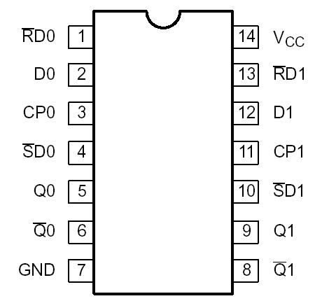
3. The input and output voltage ratings may be exceeded if the input and output current ratings are observed.DescriptionThe 74ABT5074 is a dual positive edge-triggered D-type flip-flop featuring individual data, clock, set and reset inputs; also true and complementary outputs.
Set (SDn) and reset (RDn) of the 74ABT5074 are asynchronous active low inputs and operate independently of the clock (CPn) input. Data must be stable just one setup time prior to the low-to-high transition of the clock for guaranteed propagation delays.
Clock triggering occurs at a voltage level and is not directly related to the transition time of the positive-going pulse. Following the hold time interval, data at the Dn input may be changed without affecting the levels of the output.
The 74ABT5074 is designed so that the outputs can never display a metastable state due to setup and hold time violations. If setup time and hold time are violated the propagation delays may be extended beyond the specifications but the outputs will not glitch or display a metastable state. Typical metastability parameters for the 74ABT5074 are:t = 94ps and T
o = 1.3 × 10
7 sec
where trepresents a function of the rate at which a latch in a metastable state resolves that condition and T0 represents a function of the measurement of the propensity of a latch to enter a metastable state.

 74ABT5074 Data Sheet
