SeekIC No. : 004248737
Detail
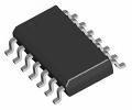
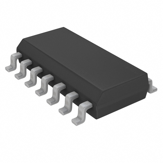
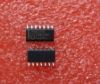
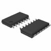
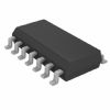
74ABT377A: Features: •Ideal for addressable register applications•8-bit positive edge-triggered register•Enable for address and data synchronization applications•Output capability: +64m...
 74ABT377A Data Sheet
floor Price/Ceiling Price
- Part Number:
- 74ABT377A
- Supply Ability:
- 5000
Price Break
- Qty
- 1~5000
- Unit Price
- Negotiable
- Processing time
- 15 Days
SeekIC Buyer Protection PLUS - newly updated for 2013!
- Escrow Protection.
- Guaranteed refunds.
- Secure payments.
- Learn more >>
Month Sales
268 Transactions
Payment Methods
All payment methods are secure and covered by SeekIC Buyer Protection PLUS.
Notice: When you place an order, your payment is made to SeekIC and not to your seller. SeekIC only pays the seller after confirming you have received your order. We will also never share your payment details with your seller.