Features: Combines D-Type latches and D-Type flip-flops for operation in transparent, latched, or clocked mode
Flow-through architecture optimizes PCB layout
Guaranteed latch-up protection
High impedance glitch free bus loading during entire power up and power down cycle
Non-destructive hot insertion capabilityPinout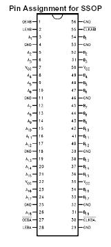 SpecificationsStorage Temperature -65°C to +150°C
Ambient Temperature under Bias -55°C to +125°C
Junction Temperature under Bias -55°C to +150°C
VCC Pin Potential to
Ground Pin -0.5V to +7.0V
Input Voltage (Note 5) -0.5V to +7.0V
Input Current (Note 5) -30 mA to +5.0 mA
Voltage Applied to Any Output
in the Disabled or
Power-off State -0.5V to 5.5V
in the HIGH State -0.5V to VCC
Current Applied to Output
in LOW State (Max) twice the rated IOL (mA)
DC Latchup Source Current -500 mA
Over Voltage Latchup (I/O) 10V
Description The 74ABT16500 18-bit universal bus transceiver combines D-type latches and D-type flip-flops to allow data flow in transparent, latched, and clocked modes.
Data flow in each direction is controlled by output-enable (OEAB and and OEBA ), latch-enable (LEAB and LEBA), and clock (CLKAB and CLKBA) inputs. For A-to-B data flow, the device operates in the transparent mode when LEAB is HIGH. When LEAB is LOW, the A data is latched if CLKAB is held at a HIGH or LOW logic level. If LEAB is LOW, the A bus data is stored in the latch/flip-flop on the HIGH-to-LOW transition of CLKAB. Output-enable OEAB is active-high. When OEAB is HIGH, the outputs are active. When OEAB is LOW, the outputs are in the high-impedance state.
Data flow for B to A is similar to that of A to B but uses OEBA , LEBA, and CLKBA . The output of the 74ABT16500 enables are complementary (OEAB is active HIGH and OEBA is active LOW).
To ensure the high-impedance state during power up or power down, OE should be tied to GND through a pulldown resistor; the minimum value of the resistor is determined by the current-sourcing capability of the driver.

 74ABT16500 Data Sheet