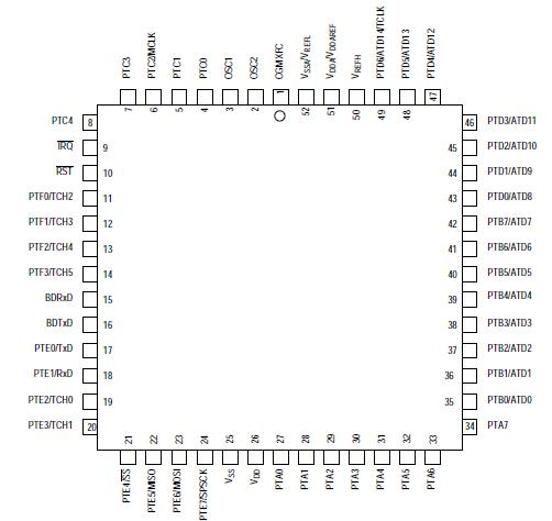
Features: Features of the MC68HC08AS32 include:
• High-performance M68HC08 architecture
• Fully upward-compatible object code with M6805, M146805, and M68HC05 Families
• 8.4-MHz internal bus frequency
• 32,256 bytes of read-only memory (ROM)
• ROM data security
• 512 bytes of on-chip electrically erasable programmable read-only memory (EEPROM)
• 1024 bytes of on-chip random-access memory (RAM)
• Serial peripheral interface module (SPI)
• Serial communications interface module (SCI)
• 16-bit, 6-channel timer interface module (TIM)
• Clock generator module (CGM)
• 8-bit, 15-channel analog-to-digital converter module (ADC)
• SAE J1850 byte data link controller digital module (BDLC-D)
• System protection features:
Computer operating properly (COP) with optional reset
Low-voltage detection with optional reset
Illegal opcode detection with optional reset
Illegal address detection with optional reset
• Low-power design (fully static with stop and wait modes)
• Master reset pin and power-on reset
Features of the CPU08 include:
• Enhanced HC05 programming model
• Extensive loop control functions
• 16 addressing modes (eight more than the HC05)
• 16-bit index register and stack pointer
• Memory-to-memory data transfers
• Fast 8 ´ 8 multiply instruction
• Fast 16/8 divide instruction
• Binary-coded decimal (BCD) instructions
• Optimization for controller applications
• C language support Applicationdeliver the application program to Motorola in one of these:
• Macintosh®1 3 1/2-inch diskette (double-sided 800 K or double-sided high-density 1.4 M)
• MS-DOS®2 or PC-DOSTM3 3 1/2-inch diskette (double-sided 720 K or double-sided high-density 1.44 M)
• MS-DOS® or PC-DOSTM 5 1/4-inch diskette (double-sided double-density 360 K or double-sided high-density 1.2 M)
Use positive logic for data and addresses.When submitting the application program on a diskette, clearly label the
diskette with this information:
• Customer name
• Customer part number
• Project or product name
• File name of object code
• Date
• Name of operating system that formatted diskette
• Formatted capacity of diskette
Pinout Specifications
Maximum ratings are the extreme limits to which the MCU can be exposed without permanently damaging it.
The MCU contains circuitry to protect the inputs against damage from high static voltages; however, do not apply voltages higher than those shown in the table below. Keep VIN and VOUT within the range VSS (VIN or VOUT) VDD. Connect unused inputs to the appropriate voltage level, either VSS or VDD
|
Rating |
Symbol |
Value |
Unit |
| Supply voltage |
VDD |
0.3 to +6.0 |
V |
| Input voltage |
VIn |
VSS 0.3
to VDD +0.3 |
V |
Maximum current per pin
excluding VDD and VSS |
I |
±25 |
mA |
| Storage temperature |
TSTG |
55 to +150 |
°C |
| Maximum current out of VSS |
IMVSS |
100 |
mA |
| Maximum current into VDD |
IMVDD |
100 |
mA |
| Reset IRQ input voltage |
VHI |
VDD to VDD + 2 |
°C |
Operating temperature range
|
TA |
-40to105
|
°C |
| Operating voltage range |
VDD |
5.0 ± 10% |
V |
Thermal resistance
PLCC (52 pins)
|
JA |
50 |
°C/W |
| I/O pin power dissipation |
PI/O |
User determined |
W |
| Power dissipation(1) |
PD |
PD = (IDD x VDD) +
PI/O = K/(TJ + 273°C) |
W |
| Constant(2) |
K |
PD x (TA + 273°C)
+ (PD 2 x JA) |
W/°C |
| Average junction temperature |
TJ |
TA = PD * JA |
°C |
| Maximum junction temperature |
TJM |
150 |
°C |
1. Power dissipation is a function of temperature.
2. K is a constant unique to the device. K can be determined from a known TA and measured PD. With this value of K, PD and TJ can be determined for any value of TA.DescriptionMotorola reserves the right to make changes without further notice to any products herein to improve reliability, function or design. Motorola does not assume any liability arising out of the application or use of any product or circuit described herein; neither does it convey any license under its patent rights nor the rights of others. Motorola products are not designed, intended, or authorized for use as components in systems intended for surgical implant into the body, or other applications intended to support or sustain life, or for any other application in which the failure of the Motorola product could create a situation where personal injury or death may occur. Should Buyer purchase or use Motorola products for any such unintended or unauthorized application, Buyer shall indemnify and hold Motorola and its officers, employees, subsidiaries, affiliates,and distributors harmless against all claims, costs, damages, and expenses, and reasonable attorney fees arising out of, directly or indirectly, any claim of personal injury or death associated with such unintended or unauthorized use, even if such claim alleges that Motorola was negligent regarding the design or manufacture of the part.

 68HC08AS32 Data Sheet


