Manufacturer: Capital Advanced Technologies
Proto Board Type: SMD to SIP Pins
Hole Diameter: -
Board Thickness: 0.031" (0.79mm) 1/32"
Material: -
Series: 6000, Surfboards®
Package Accepted: SOT-23
Number of Positions: 20
Size / Dimension: 0.50" x 2.00" (12.7mm x 50.8mm)
Features: • Fast match times: 3.5, 3.8, 4.0 and 4.5ns
• Fast clock speed: 166, 150, 133, and 100MHz
• Fast OE# access times: 3.5, 3.8, 4.0 and 5.0ns
• Pipelined data comparator
• Data input register load control by DEN#
• Optimal for depth expansion (one cycle chip deselect to liminate bus contention)
• 3.3V -5% and +10% core power supply
• 2.5V or 3.3V I/O supply
• 5V tolerant inputs except I/O's
• Clamp diodes to VSS at all inputs and outputs
• Common data inputs and data outputs
• JTAG boundary scan
• BYTE WRITE ENABLE and GLOBAL WRITE control
• Three chip enables for depth expansion and address ipeline
• Address, data and control registers
• Internally self-timed WRITE CYCLE
• Burst control pins (interleaved or linear burst sequence)
• Automatic power-down for portable applications
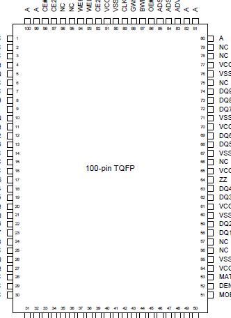
• Low profile 119 lead, 14mm x 22mm BGA (Ball Grid rray) and JEDEC standard 100 pin TQFP packagesPinout Specifications
Voltage on VCC Supply Relative to VSS........ -5V to +4.6V
VIN .......................................................... -0.5V to VCC+0.5V
Storage Temperature (plastic) .......................-55oC to +150o
Junction Temperature ...................................................+150o
Power Dissipation ...........................................................1.0W
Short Circuit Output Current ..........................................50mA
*Stresses greater than those listed uunder "Absolute Maximum atings" may cause permanent damage to the device.This is a stress ating only and functional operation of the device at these or any ther conditions above those indicated in the operational sections of his specification is not implied. Exposure to absolute maximum ating conditions for extended periods may affect reliability.
DescriptionThe Galvantech Synchronous Burst SRAM family of 6520 mploys high-speed, low power CMOS designs using dvanced triple-layer polysilicon, double-layer metal echnology. Each memory cell consists of four transistors and wo high valued resistors.
All synchronous inputs of 6520 are gated by registers controlled y a positive-edge-triggered clock input (CLK). The ynchronous inputs include all addresses, all data inputs, ddress-pipelining chip enable (CE#), depth-expansion chip nables (CE2# and CE2), burst control inputs (ADSC#, DSP#, and ADV#), write enables (WEL#, WEH#, and WE#), global write (GW#), and data input enable (DEN#). synchronous inputs include the burst mode control MODE), the output enable (OE#) and the match output nable (MOE#). The data outputs (Q) and match output MATCH), enabled by OE# and MOE# respectively, are also synchronous.
ddresses and chip enables of 6520 are registered with either ddress status processor (ADSP#) or address status controller ADSC#) input pins. Subsequent burst addresses can be nternally generated as controlled by the burst advance pin ADV#).
Data inputs of 6520 are registered with data input enable (DEN#) nd chip enable pins (CE#, CE2 and CE2#). The outputs of he data input registers are compared with data in the memory rray and a match signal is generated. The match output is ated into a pipeline register and released to the match output in at the next rising edge of clock (CLK).
Address, data inputs, and write controls of 6520 are registered onchip o initiate self-timed WRITE cycle. WRITE cycles can e one to two bytes wide as controlled by the write control nputs. Individual byte write allows individual byte to be ritten. WEL# controls DQ1-DQ9. WEH# controls DQ10- Q18. WEL#, and WEH# can be active only with BWE# eing LOW. GW# being LOW causes all bytes to be written.
The 6520 operates from a +3.3V power supply ith output power supply being +2.5V or +3.3V. All inputs nd outputs are LVTTL compatible. The device is ideally uited for address tag RAM for up to 8MB secondary cache.
Parameters: | Technical/Catalog Information | 6520 |
| Vendor | Paladin Tools |
| Category | Tools |
| For Use With/Related Products | Datacomm, telecom, and electrical installations |
| Tool Type | Multi-tool |
| Lead Free Status | Lead Not Applicable |
| RoHS Status | RoHS Not Applicable |
| Other Names | 6520
6520
PAL6520 ND
PAL6520ND
PAL6520
|

 6520 Data Sheet


