54F646

Features: *Independent registers for A and B buses*Multiplexed real-time and stored data*74F648 has inverting data paths*74F646/74F646B have non-inverting data paths*74F646B is a faster version of the 74F646*3-STATE outputs*300 mil slim DIPPinoutSpecificationsStorage Temperature .....................

product image

54F646 Picture
SeekIC No. : 004233311 Detail

54F646: Features: *Independent registers for A and B buses*Multiplexed real-time and stored data*74F648 has inverting data paths*74F646/74F646B have non-inverting data paths*74F646B is a faster version of t...

floor Price/Ceiling Price

Part Number:
54F646
Supply Ability:
5000

Price Break

  • Qty
  • 1~5000
  • Unit Price
  • Negotiable
  • Processing time
  • 15 Days
Total Cost: $ 0.00

SeekIC Buyer Protection PLUS - newly updated for 2013!

  • Escrow Protection.
  • Guaranteed refunds.
  • Secure payments.
  • Learn more >>

Month Sales

268 Transactions

Rating

evaluate  (4.8 stars)

Upload time: 2024/5/29

Payment Methods

All payment methods are secure and covered by SeekIC Buyer Protection PLUS.

Notice: When you place an order, your payment is made to SeekIC and not to your seller. SeekIC only pays the seller after confirming you have received your order. We will also never share your payment details with your seller.
Product Details

Description


Features:

*Independent registers for A and B buses
*Multiplexed real-time and stored data
*74F648 has inverting data paths
*74F646/74F646B have non-inverting data paths
*74F646B is a faster version of the 74F646
*3-STATE outputs
*300 mil slim DIP


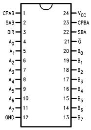
Pinout

  Connection Diagram


Specifications

Storage Temperature .........................−65°C to +150°C
Ambient Temperature under Bias....... −55°C to +125°C
Junction Temperature under Bias .......−55°C to +175°C
                        Plastic .........................−65°C to +150°C
VCC Pin Potential to Ground Pin............... −0.5V to +7.0V
Input Voltage (Note 2)............................. −0.5V to +7.0V
Input Current (Note 2) ......................−30 mA to +5.0 mA
Voltage Applied to Output
   in HIGH State (with VCC = 0V)
   Standard Output .......................................−0.5V to VCC
   TRI-STATE Output....................................−0.5V to +5.5V
Current Applied to Output
   in LOW State (Max)..................twice the rated IOL (mA)
ESD Last Passing Voltage (Min) .............................4000V


Description

    These 54F646 consist of bus transceiver circuits with TRI- STATE, D-type flip-flops, and control circuitry arranged for multiplexed transmission of data directly from the input bus or from the internal registers. Data on the A or B bus will be clocked into the registers as the appropriate clock pin goes to a high logic level. Control G and direction pins are provided to control the transceiver function. In the transceiver mode, data present at the high impedance port may be stored in either the A or the B register or in both. The select controls of 54F646 can multiplex stored and real-time (transparent mode) data. The direction control determines which bus will receive data when the enable control G is Active LOW. In the isolation mode (control G HIGH), A data of 54F646 may be stored in the B register and/or B data may be stored in the A register.


Customers Who Bought This Item Also Bought

Margin,quality,low-cost products with low minimum orders. Secure your online payments with SeekIC Buyer Protection.
Transformers
Resistors
Cables, Wires - Management
Inductors, Coils, Chokes
Prototyping Products
DE1
View more