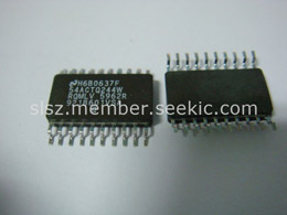
54ACTQ646

Features: · Guaranteed simultaneous switching noise level and dynamic threshold performance· Independent registers for A and B busses· Multiplexed real-time and stored data transfers· 300 mil slim dual-in-line package· Outputs source/sink 24 mA· Faster prop delays than the standard AC/ACT646· 4 kV...

product image

54ACTQ646 Picture
SeekIC No. : 004233226 Detail

54ACTQ646: Features: · Guaranteed simultaneous switching noise level and dynamic threshold performance· Independent registers for A and B busses· Multiplexed real-time and stored data transfers· 300 mil slim d...

floor Price/Ceiling Price

Part Number:
54ACTQ646
Supply Ability:
5000

Price Break

  • Qty
  • 1~5000
  • Unit Price
  • Negotiable
  • Processing time
  • 15 Days
Total Cost: $ 0.00

SeekIC Buyer Protection PLUS - newly updated for 2013!

  • Escrow Protection.
  • Guaranteed refunds.
  • Secure payments.
  • Learn more >>

Month Sales

268 Transactions

Rating

evaluate  (4.8 stars)

Upload time: 2024/5/22

Payment Methods

All payment methods are secure and covered by SeekIC Buyer Protection PLUS.

Notice: When you place an order, your payment is made to SeekIC and not to your seller. SeekIC only pays the seller after confirming you have received your order. We will also never share your payment details with your seller.
Product Details

Description


Features:

· Guaranteed simultaneous switching noise level and dynamic threshold performance
· Independent registers for A and B busses
· Multiplexed real-time and stored data transfers
· 300 mil slim dual-in-line package
· Outputs source/sink 24 mA
· Faster prop delays than the standard AC/ACT646
· 4 kV minimum ESD immunity
· Standard Microcircuit Drawing (SMD) 5962-9219601


Pinout

  Connection Diagram


Specifications

Supply Voltage (VCC) ........−0.5V to +7.0V
DC Input Diode Current (IIK)
VI = −0.5V ...................−20 mA
VI = VCC + 0.5V ................+20 mA
DC Input Voltage (VI) ......−0.5V to VCC0.5V
DC Output Diode Current (IOK)
VO = −0.5V .................. −20 mA
VO = VCC + 0.5V ...............+20 mA
DC Output Voltage (VO) ..  −0.5V to VCC + 0.5V
DC Output Source
or Sink Current (IO)..............±50 mA
DC VCC or Ground Current
per Output Pin (ICC or IGND)........ ±50 mA
Storage Temperature (TSTG).. −65°C to +150°C
DC Latch-Up Source
or Sink Current ................±300 mA
Junction Temperature (TJ)CDIP ........175°C


Description

The 54ACTQ646 consist of registered bus transceiver circuits, with outputs, D-type flip-flops, and control circuitry providing multiplexed transmission of data directly from the input bus or from the internal storage registers. Data of 54ACTQ646 on the A or B bus will be loaded into the respective registers on the LOW-to-HIGH transition of the appropriate clock pin (CPAB or CPBA). The four fundamental handling functions available are illustrated in Figures 1, 2, 3, 4.

The 54ACTQ646 utilizes FSC Quiet Series technology to guarantee quiet output switching and improved dynamic threshold performance. 54ACTQ646 features GTO™ output control and undershoot corrector in addition to a split ground bus for superior performance.


Customers Who Bought This Item Also Bought

Margin,quality,low-cost products with low minimum orders. Secure your online payments with SeekIC Buyer Protection.
Memory Cards, Modules
Discrete Semiconductor Products
Test Equipment
LED Products
Fans, Thermal Management
View more