54ACT899QCQB

Pinout DescriptionThe 54ACT899QCQB is designed as a 9-bit to 9-bit parity transceiver with transparent latched. The device can operate as a feed-through transceiver or it can generate/check parity from the 8-bit data busses in either direction.54ACT899QCQB has nine features. (1)Latchable transcei...

product image

54ACT899QCQB Picture
SeekIC No. : 004233204 Detail

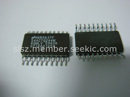
54ACT899QCQB: Pinout DescriptionThe 54ACT899QCQB is designed as a 9-bit to 9-bit parity transceiver with transparent latched. The device can operate as a feed-through transceiver or it can generate/check parity ...

floor Price/Ceiling Price

Part Number:
54ACT899QCQB
Supply Ability:
5000

Price Break

  • Qty
  • 1~5000
  • Unit Price
  • Negotiable
  • Processing time
  • 15 Days
Total Cost: $ 0.00

SeekIC Buyer Protection PLUS - newly updated for 2013!

  • Escrow Protection.
  • Guaranteed refunds.
  • Secure payments.
  • Learn more >>

Month Sales

268 Transactions

Rating

evaluate  (4.8 stars)

Upload time: 2025/3/13

Payment Methods

All payment methods are secure and covered by SeekIC Buyer Protection PLUS.

Notice: When you place an order, your payment is made to SeekIC and not to your seller. SeekIC only pays the seller after confirming you have received your order. We will also never share your payment details with your seller.
Product Details

Description


Pinout

  Connection Diagram


Description

The 54ACT899QCQB is designed as a 9-bit to 9-bit parity transceiver with transparent latched. The device can operate as a feed-through transceiver or it can generate/check parity from the 8-bit data busses in either direction.

54ACT899QCQB has nine features. (1)Latchable transceiver with output sink of 24mA. (2)Option to select generate parity and cheak or "feed-through" data/parity in directions A-to-B or B-to-A. (3)Independent latch enable for A-to-B and B-to-A directions. (4)Select pin for ODD/EVEN parity. (5)/ERRA and /ERRB output pins for parity checking. (6)Ability to simultaneously generate and check parity. (7)May be used in system applications in place of the '280. (8)May be used in system applications in place of the '657 and '373 (no need to change T/R to check parity). (9)4kV minimum ESD immunity. Those are all the main features.

Some absolute maximum ratings of 54ACT899QCQB have been concluded into several points as follow. (1)Its supply voltage would be from -0.5V to 7.0V. (2)Its DC input diode current would be -20mA at Vi=-0.5V and would be +20mA at Vi=Vdd+0.5V. (3)Its DC input voltage would be from -0.5V to Vcc+0.5V. (4)Its DC output diode current would be -20mA at Vo=-0.5V and would be +20mA at Vo=Vcc+0.5V. (5)Its DC output voltage would be from -0.5V to Vcc+0.5V. (6)Its DC output source or sink current would be +/-50mA. (7)Its DC Vcc or ground current per output pin would be +/-50mA. (8)Its storage temperature range would be from -65°C to 150°C. (9)Its DC latch-up source or sink current would be +/-300mA. (10)Its junction temperature would be 175°C for CDIP and would be 140°C for PDIP. 54ACT899QCQB should be noted that stresses above those listed in absolute maximum ratings may cause permanent damage to device.

Also some electrical characteristics of 54ACT899QCQB at Vcc=3.0V are concluded as follow. (1)Its minimum high level input voltage would be min 2.1V. (2)Its maximum low level input voltage would be max 0.9V. (3)Its minimum high level output voltage would be min 2.9V. (4)Its maximum low level output voltage would be max 0.1V. And so on. If you have any question or suggestion or want to know more information about 54ACT899QCQB please contact us for details. Thank you!


Customers Who Bought This Item Also Bought

Margin,quality,low-cost products with low minimum orders. Secure your online payments with SeekIC Buyer Protection.
Audio Products
Cable Assemblies
Optoelectronics
Fans, Thermal Management
Boxes, Enclosures, Racks
View more