Features: ` ICC and IOZ reduced by 50%
` Outputs source/sink 24 mA
` 'ACT157 has TTL-compatible inputs
` Standard Microcircuit Drawing (SMD)
-'AC157: 5962-89539
-'ACT157: 5962-89688
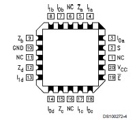
Pinout Specifications
| Temperature Min |
-55 deg C |
| Temperature Max |
125 deg C |
| View Using Catalog |
If Military/Aerospace specified devices are required,please contact the National Semiconductor Sales ffice/Distributors for availability and specifications.
Supply Voltage (VCC) ..................................−0.5V to +7.0V
DC Input Diode Current (IIK)
VI = −0.5V ..............................................................−20 mA
VI = VCC + 0.5V ......................................................+20 mA
DC Input Voltage (VI) .........................−0.5V to VCC + 0.5V
DC Output Diode Current (IOK)
VO = −0.5V .............................................................−20 mA
VO = VCC + 0.5V .....................................................+20 mA
DC Output Voltage (VO) ......................−0.5V to VCC + 0.5V
DC Output Source
or Sink Current (IO) ................................................±50 mA
DC VCC or Ground Current
per Output Pin (ICC or IGND) ...................................±50 mA
Storage Temperature (TSTG) .....................−65 to +150
Junction Temperature (TJ)
CDIP ...........................................................................175
Supply Voltage (VCC)
'AC ..................................................................2.0V to 6.0V
'ACT ................................................................4.5V to 5.5V
Input Voltage (VI) ................................................0V to VCC
Output Voltage (VO) ............................................0V to VCC
Operating Temperature (TA)
54AC/ACT ..................................................−55 to +125
Minimum Input Edge Rate (DV/Dt)
'AC Devices
VIN from 30% to 70% of VCC
VCC @ 3.3V, 4.5V, 5.5V ......................................125 mV/ns
Minimum Input Edge Rate (DV/Dt)
'ACT Devices
VIN from 0.8V to 2.0V
VCC @ 4.5V, 5.5V ...............................................125 mV/ns
Note 1: Absolute maximum ratings are those values beyond which damage to the device may occur. The databook specifications should be met, without exception, to ensure that the system design is reliable over its power supply,temperature, and output/input loading variables. National does not recommend operation of FACT™ circuits outside databook specifications.
DescriptionThe 54ACT157 is a high-speed quad 2-input multiplexer. Four bits of data from two sources can be selected using the common Select and Enable inputs. The four outputs present the selected data in the true (noninverted) form. The 54ACT157 can also be used as a function generator.
More Application Notes
| Title |
Size in Kbytes |
Date |
|
| AN-925: Radiation Design Test Data for Advanced CMOS Product |
194 Kbytes |
5-Aug-95 |
Download |
If you have trouble printing or viewing PDF file(s), see Printing Problems.
|
The 54ACT157 is a high-speed quad 2-input multiplexer.
Four bits of data from two sources can be selected using the common Select and Enable inputs. The four outputs present the selected data in the true (noninverted) form. The 54ACT157 can also be used as a function generator.

 54ACT157 Data Sheet


