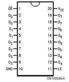
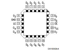
Features: ` ICC and IOZ reduced by 50%`Eight latches in a single package`TRI-STATE outputs for bus interfacing` Outputs source/sink 24 mA` 'ACT373 has TTL-compatible inputs`Standard Microcircuit Drawing (SMD)- 'AC373: 5962-87555- 'ACT373: 5962-87556PinoutSpecifications Temperature Min -55 de...
54AC373: Features: ` ICC and IOZ reduced by 50%`Eight latches in a single package`TRI-STATE outputs for bus interfacing` Outputs source/sink 24 mA` 'ACT373 has TTL-compatible inputs`Standard Microcircuit Dra...
SeekIC Buyer Protection PLUS - newly updated for 2013!
268 Transactions
All payment methods are secure and covered by SeekIC Buyer Protection PLUS.
Temperature Min | -55 deg C |
Temperature Max | 125 deg C |
View Using Catalog |
If Military/Aerospace specified devices are required, please contact the National Semiconductor Sales Office/Distributors for availability and specifications.
Supply Voltage (VCC)........... −0.5V to +7.0V
DC Input Diode Current (IIK)
VI = −0.5V ................ ....−20 mA
VI = VCC + 0.5V.................. +20 mA
DC Input Voltage (VI) .........−0.5V to VCC + 0.5V
DC Output Diode Current (IOK)
VO = −0.5V..................... −20 mA
VO = VCC + 0.5V.............. .... +20 mA
DC Output Voltage (VO) ........−0.5V to VCC + 0.5V
DC Output Source
or Sink Current (IO) .................±50 mA
DC VCC or Ground Current
per Output Pin (ICC or IGND) .............±50 mA
Storage Temperature (TSTG) .......−65°C to +150°C
Junction Temperature (TJ)
CDIP.......................... 175°C
to the device may occur. The databook specifications should be met, without exception, to ensure that the system design is reliable over its power supply, temperature, and output/input loading variables. National does not recommend operation of FACT® circuits outside databook specifications.
The 54AC373 consists of eight latches with TRI-STATE outputs for bus organized system applications. The flip-flops 54AC373 appear transparent to the data when Latch Enable (LE) is HIGH. When LE is LOW, the data that meets the setup time is latched. Data appears on the bus when the Output Enable (OE#) is LOW. When OE# is HIGH, the bus output is in the high impedance state.
More Application Notes
Title | Size in Kbytes | Date | |
AN-932: SEU and Latch Up Tolerant Advanced CMOS Technology | 186 Kbytes | 5-Jan-96 | Download |
AN-925: Radiation Design Test Data for Advanced CMOS Product | 194 Kbytes | 5-Aug-95 | Download |
If you have trouble printing or viewing PDF file(s), see Printing Problems. |
The 54AC373 consists of eight latches with TRI-STATE outputs for bus organized system applications. The flip-flops appear transparent to the data when Latch Enable (LE) is HIGH. When LE is LOW, the data that meets the setup time is latched. Data appears on the bus when the Output Enable (OE) is LOW. WhenOE is HIGH, the bus output of 54AC373 is in the high impedance state.