Features: ` Ideal buffer for microprocessor or memory
` Eight edge-triggered D flip-flops
` Buffered common clock
` Buffered, asynchronous master reset
` See '377 for clock enable version
` See '373 for transparent latch version
` See '374 for TRI-STATE® version
` Outputs source/sink 24 mA
` 'ACT has TTL-compatible inputs
` Standard Military Drawing (SMD)
-'AC273: 5962-87756Pinout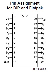 SpecificationsIf Military/Aerospace specified devices are required, please contact the National Semiconductor Sales Office/ Distributors for availability and specifications.
Supply Voltage (VCC) −0.5V to +7.0V
DC Input Diode Current (IIK)
VI = −0.5V −20 mA
VI = VCC + 0.5V +20 mA
DC Input Voltage (VI) −0.5V to VCC + 0.5V
DC Output Diode Current (IOK)
VO = −0.5V −20 mA
VO = VCC + 0.5V+20 mA
DC Output Voltage (VO) −0.5V to to VCC + 0.5V
DC Output Source
or Sink Current (IO) ±50 mA
DC VCC or Ground Current
per Output Pin (ICC or IGND)±50 mA
Storage Temperature (TSTG) −65°C to +150°C
Junction Temperature (TJ)
CDIP 175°C
Note 1: Absolute maximum ratings are those values beyond which damage to the device may occur. The databook specifications should be met, without exception, to ensure that the system design is reliable over its power supply, temperature, and output/input loading variables. National does not recommend operation of FACT™ circuits outside databook specifications.
| Temperature Min |
-55 deg C |
| Temperature Max |
125 deg C |
| View Using Catalog |
DescriptionThe 54AC273 has eight edge-triggered D-type flip-flops with individual D inputs and Q outputs. The common buffered Clock (CP) and Master Reset (
MR) input load and reset (clear) all flip-flops simultaneously.
The register 54AC273 is fully edge-triggered. The state of each D input, one setup time before the LOW-to-HIGH clock transition, is transferred to the corresponding flip-flop's Q output.
All outputs of 54AC273 will be forced LOW independently of Clock or Data inputs by a LOW voltage level on the
MR input. The device is useful for applications where the true output only is required and the Clock and Master Reset are common to all storage elements.
The 54AC273 has eight edge-triggered D-type flip-flops with individual D inputs and Q outputs. The common buffered Clock (CP) and Master Reset (MR#) input load and reset (clear) all flip-flops simultaneously.
The register 54AC273 is fully edge-triggered. The state of each D input, one setup time before the LOW-to-HIGH clock transition, is transferred to the corresponding flip-flop's Q output.
All outputs of 54AC273 will be forced LOW independently of Clock or Data inputs by a LOW voltage level on the MR# input. The device is useful for applications where the true output only is required and the Clock and Master Reset are common to all storage elements.
Application Notes
| Title |
Size in Kbytes |
Date |
|
| AN-925: Radiation Design Test Data for Advanced CMOS Product |
194 Kbytes |
5-Aug-95 |
Download |
If you have trouble printing or viewing PDF file(s), see Printing Problems.
|

 54AC273 Data Sheet