54AC175F_1354730

Features: ` Edge-triggered D-type inputs` Buffered positive edge-triggered clock` Asynchronous common reset` True and complement output` Outputs source/sink 24 mA` 'ACT175 has TTL-compatible inputs` Standard Microcircuit Drawing (SMD) -'AC175: 5962-89552 -'ACT175: 5962-89693PinoutSpecificationsIf ...

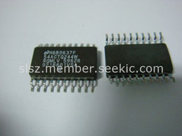
product image

54AC175F_1354730 Picture
SeekIC No. : 004233091 Detail

54AC175F_1354730: Features: ` Edge-triggered D-type inputs` Buffered positive edge-triggered clock` Asynchronous common reset` True and complement output` Outputs source/sink 24 mA` 'ACT175 has TTL-compatible inputs`...

floor Price/Ceiling Price

Part Number:
54AC175F_1354730
Supply Ability:
5000

Price Break

  • Qty
  • 1~5000
  • Unit Price
  • Negotiable
  • Processing time
  • 15 Days
Total Cost: $ 0.00

SeekIC Buyer Protection PLUS - newly updated for 2013!

  • Escrow Protection.
  • Guaranteed refunds.
  • Secure payments.
  • Learn more >>

Month Sales

268 Transactions

Rating

evaluate  (4.8 stars)

Upload time: 2024/12/25

Payment Methods

All payment methods are secure and covered by SeekIC Buyer Protection PLUS.

Notice: When you place an order, your payment is made to SeekIC and not to your seller. SeekIC only pays the seller after confirming you have received your order. We will also never share your payment details with your seller.
Product Details

Description


Features:

` Edge-triggered D-type inputs
` Buffered positive edge-triggered clock
` Asynchronous common reset
` True and complement output
` Outputs source/sink 24 mA
` 'ACT175 has TTL-compatible inputs
` Standard Microcircuit Drawing (SMD)
     -'AC175: 5962-89552
     -'ACT175: 5962-89693


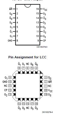
Pinout

  Connection Diagram


Specifications

If Military/Aerospace specified devices are required, please contact the National Semiconductor Sales Office/Distributors for availability and specifications.
Supply Voltage (VCC)                                           −0.5V to +7.0V
DC Input Diode Current (IIK)
VI = −0.5V                                                           −20 mA
VI = VCC + 0.5V                                                   +20 mA
DC Input Voltage (VI)                                          −0.5V to VCC + 0.5V
DC Output Diode Current (IOK)
VO = −0.5V                                                          −20 mA
VO = VCC + 0.5V                                                  +20 mA
DC Output Voltage (VO)                                       −0.5V to VCC + 0.5V
DC Output Source
or Sink Current (IO)                                             ±50 mA
DC VCC or Ground Current
per Output Pin (ICC or IGND)                                ±50 mA
Storage Temperature (TSTG)                                −65°C to +150°C
Junction Temperature (TJ)
CDIP                                                                     175°C


Description

The 54AC175F_1354730 is a high-speed quad D flip-flop. The device is useful for general flip-flop requirements where clock and clear inputs are common. The information on the D inputs is stored during the LOW-to-HIGH clock transition. Both true and complemented outputs of each flip-flop 54AC175F_1354730 are provided. A Master Reset input resets all flip-flops, independent of the Clock or D inputs, when LOW.


Customers Who Bought This Item Also Bought

Margin,quality,low-cost products with low minimum orders. Secure your online payments with SeekIC Buyer Protection.
Optoelectronics
Isolators
Hardware, Fasteners, Accessories
Programmers, Development Systems
Cable Assemblies
View more