54AC16823

Features: Members of the Texas Instruments WidebusTM FamilyProvides Extra Data Width Necessary for Wider Address/Data Paths or Buses With ParityFlow-Through Architecture Optimizes PCB LayoutDistributed VCC and GND Pin Configuration Minimizes High-Speed Switching NoiseEPICTM (Enhanced-Performance I...

product image

54AC16823 Picture
SeekIC No. : 004233087 Detail

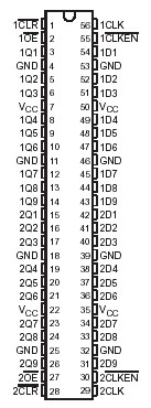
54AC16823: Features: Members of the Texas Instruments WidebusTM FamilyProvides Extra Data Width Necessary for Wider Address/Data Paths or Buses With ParityFlow-Through Architecture Optimizes PCB LayoutDistribu...

floor Price/Ceiling Price

Part Number:
54AC16823
Supply Ability:
5000

Price Break

  • Qty
  • 1~5000
  • Unit Price
  • Negotiable
  • Processing time
  • 15 Days
Total Cost: $ 0.00

SeekIC Buyer Protection PLUS - newly updated for 2013!

  • Escrow Protection.
  • Guaranteed refunds.
  • Secure payments.
  • Learn more >>

Month Sales

268 Transactions

Rating

evaluate  (4.8 stars)

Upload time: 2024/6/9

Payment Methods

All payment methods are secure and covered by SeekIC Buyer Protection PLUS.

Notice: When you place an order, your payment is made to SeekIC and not to your seller. SeekIC only pays the seller after confirming you have received your order. We will also never share your payment details with your seller.
Product Details

Description


Features:

 Members of the Texas Instruments Widebus TM Family
 Provides Extra Data Width Necessary for Wider Address/Data Paths or Buses With Parity
 Flow-Through Architecture Optimizes PCB Layout
 Distributed VCC and GND Pin Configuration Minimizes High-Speed Switching Noise
 EPIC TM (Enhanced-Performance Implanted CMOS) 1-m Process
 500-mA Typical Latch-Up Immunity at 125°C
 Package Options Include Plastic 300-mil Shrink Small-Outline (DL) Package Using 25-mil Center-to-Center Pin Spacings and 380-mil Fine-Pitch Ceramic Flat (WD) Package Using 25-mil Center-to-Center Pin Spacings


Pinout

  Connection Diagram


Specifications

Supply voltage range, VCC . . . . . . . . . . . . . . . . . . . . . . . . . . . . . . . . . . . . . . . . . . . . . .0.5 V to 7 V
Input voltage range, VI (see Note 1) . . . . . . . . . . . . . . . . . . . . . . . . . . .. . . . .0.5 V to VCC + 0.5 V
Output voltage range, VO (see Note 1) . . . . . . . . . . . . . . . . . . . . . . . . . . . . . .0.5 V to VCC + 0.5 V
Input clamp current, IIK (VI < 0 or VI > VCC) . . . . . . . . . . . . . . . . . . . . . . . . . . . .. . . . . . . . . .±20 mA
Output clamp current, IOK (VO < 0 or VO > VCC) . . . . . . . . . . . . . . . . . . . . . . . . . . . . . . . . . . ±50 mA
Continuous output current, IO (VO = 0 to VCC) . . . . . . . . . . . . . . . . . . . . . . . . . . . . .. . . . . . .±50 mA
Continuous current through VCC or GND  . . . . . . . . . . . . . . . . . . . . . . . . . . . . . . . . . . . . . ... ±450mA
Maximum power package dissipation at TA = 55°C (in still air)(see Note 2): DL package . .. . . 1.4 W
Storage temperature range ,Tstg . . . . . . . . . . . . . . . . . . . . . . . . . . . . . . . . . .. . . . . .65°C to 150°C 


Description

These 54AC16823 18-bit flip-flops feature 3-state outputs designed specifically for driving highly capacitive or relatively low-impedance loads. They are particularly suitable for implementing wider buffer registers, I/O ports, parity bus interfacing, and working registers.

The 54AC16823 can be used as two 9-bit flip-flops or one 18-bit flip-flop. With the clock-enable (CLKEN) input low, the D-type flip-flops enter data on the low-to-high transitions of the clock. Taking CLKEN high disables the clock buffer, thus latching the outputs. Taking the clear (CLR) input low causes the Q outputs to go low independently of the clock.

The output enable (OE) input of 54AC16823 can be used to place the outputs in either a normal logic state (high or low) or a high-impedance state. In the high-impedance state, the outputs neither load nor drive the bus lines significantly.

OE does not affect the internal operation of the flip-flops. Old data can be retained or new data can be entered while the outputs are in the high-impedance state.

The 74AC16823 is packaged in TI's shrink small-outline package (DL), which provides twice the I/O pin count and functionality of standard small-outline packages in the same printed-circuit-board area.

The 54AC16374 is characterized for operation over the full military temperature range of 55°C to 125°C. The 74AC16823 is characterized for operation from 40°C to 85°C.


Customers Who Bought This Item Also Bought

Margin,quality,low-cost products with low minimum orders. Secure your online payments with SeekIC Buyer Protection.
Hardware, Fasteners, Accessories
Resistors
Crystals and Oscillators
Boxes, Enclosures, Racks
View more