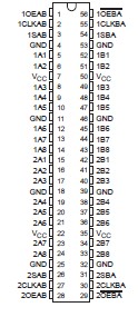
Features: ` Members of the Texas Instruments Widebus E Family` Independent Registers and Enables for A and B Buses` Multiplexed Real-Time and Stored Data` Flow-Through Architecture Optimizes PCB Layout` Distributed VCC and GND Pin Configurations Minimize High-Speed Switching Noise` EPIC E (E...
54AC16652: Features: ` Members of the Texas Instruments Widebus E Family` Independent Registers and Enables for A and B Buses` Multiplexed Real-Time and Stored Data` Flow-Through Architecture Optimizes PCB...
SeekIC Buyer Protection PLUS - newly updated for 2013!
268 Transactions
All payment methods are secure and covered by SeekIC Buyer Protection PLUS.
` Members of the Texas Instruments Widebus E Family
` Independent Registers and Enables for A and B Buses
` Multiplexed Real-Time and Stored Data
` Flow-Through Architecture Optimizes PCB Layout
` Distributed VCC and GND Pin Configurations Minimize High-Speed Switching Noise
` EPIC E (Enhanced-Performance Implanted CMOS) 1-mm Process
` 500-mA Typical Latch-Up Immunity at 125
` Package Options Include Plastic 300-mil Shrink Small-Outline (DL) Packages Using 25-mil Center-to-Center Pin Spacings and 380-mil Fine-Pitch Ceramic Flat (WD) Packages Using 25-mil Center-to-Center Pin Spacings
Supply voltage range, VCC . . . . . . . . . . . . . . . . . . . . . . . . . . . . . . . . . . . . . . . . . . . . . . . . . . . . 0.5 V to 7 V
Input voltage range, VI (see Note 1) . . . . . . . . . . . . . . . . . . . . . . . . . . . . . . . . . . . . . . 0.5 V to VCC + 0.5 V
Output voltage range, VO (see Note 1) . . . . . . . . . . . . . . . . . . . . . . . . . . . . . . . . . . . . 0.5 V to VCC + 0.5 V
Input clamp current, IIK (VI < 0 or VI > VCC) . . . . . . . . . . . . . . . . . . . . . . . . . . . . . . . . . . . . . . . . . . . ±20 mA
Output clamp current, IOK (VO < 0 or VO > VCC) . . . . . . . . . . . . . . . . . . . . . . . . . . . . . . . . . . . . . . . . . ±50 mA
Continuous output current, IO (VO = 0 to VCC) . . . . . . . . . . . . . . . . . . . . . . . . . . . . . . . . . . . . . . . . . . ±50 mA
Continuous current through VCC or GND . . . . . . . . . . . . . . . . . . . . . . . . . . . . . . . . . . . . . . . . . . . . . . ±400 mA
Maximum package power dissipation at TA = 55 (in still air) (see Note 2): DL package . . . . . . . . . . . 1.4 W
Storage temperature range, Tstg . . . . . . . . . . . . . . . . . . . . . . . . . . . . . . . . . . . . . . . . . . . . . . . 65 to 150
† Stresses beyond those listed under "absolute maximum ratings" may cause permanent damage to the device. These are stress ratings only, and functional operation of the device at these or any other conditions beyond those indicated under "recommended operating conditions" is not implied. Exposure to absolute-maximum-rated conditions for extended periods may affect device reliability.
NOTES:
1. The input and output voltage ratings may be exceeded if the input and output current ratings are bserved.
2. The maximum package power dissipation is calculated using a junction temperature of 150 and a board trace length of 750 mils.
The 54AC16652 are 16-bit bus transceivers that consist of D-type flip-flops and control circuitry arranged for multiplexed transmission of data directly from the data bus or from the internal storage registers. 54AC16652 can be used as two 8-bit transceivers or one 16-bit transceiver.
Complementary output-enable (OEAB and OEBA) inputs of 54AC16652 are provided to control the transceiver functions. Select-control (SAB and SBA) inputs are provided to select whether real-time or stored data is transferred. A low input level selects real-time data, and a high input level selects stored data. The circuitry used for select control eliminates the typical decoding glitch that occurs in a multiplexer during the transition between stored and real-time data. Figure 1 illustrates the four fundamental bus-management functions that can be performed with the 54AC16652.