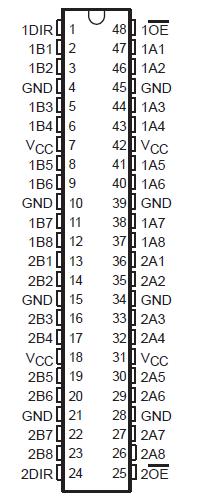
Features: ·Members of the Texas Instruments WidebusE Family
·Flow-Through Architecture Optimizes PCB Layout
·Distributed VCC and GND Pin Configuration Minimizes High-Speed Switching Noise
· EPIC™ (Enhanced-Performance Implanted CMOS) 1-mm Process
·500-mA Typical Latch-Up Immunity at 125°C
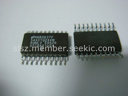
·Package Options Include Plastic 300-mil Shrink Small-Outline (DL) Packages Using 25-mil Center-to-Center Pin Spacings and 380-mil Fine-Pitch Ceramic Flat (WD) Packages Using 25-mil Center-to-Center Pin SpacingsPinout Specifications
Supply voltage range, VCC . . . . . . . . . . . . . . . . . . . . . . . . . . . . . . . . . . . . 0.5 V to 7 V
Input voltage range, VI (see Note 1) . . . . . . . . . . . . . . . . . . . . . . 0.5 V to VCC + 0.5 V
Output voltage range, VO (see Note 1) . . . . . . . . . . . . . . . . . . . .. 0.5 V to VCC + 0.5 V
Input clamp current, IIK (VI < 0 or VI > VCC) . . . . . . . . . . . . . . . . . . . . . . . . . . . ±20 mA
Output clamp current, IOK (VO < 0 or VO > VCC) . . . . . . . . . . . . . . . . . . . . . . . . ±50 mA
Continuous output current, IO (VO = 0 to VCC) . . . . . . . . . . . . . . . . . . . . . . . . . . ±50 mA
Continuous current through VCC or GND . . . . . . . . . . . . . . . . . . . . . . . . . . . . . . ±400 mA
Maximum power dissipation at TA = 55°C (in still air)(see Note 2): DL package . . 1.2 W
Storage temperature range, Tstg . . . . . . . . . . . . . . . . . . . . . . . . . . . . . 65°C to 150°C
† Stresses beyond those listed under "absolute maximum ratings" may cause permanent damage to the device. These are stress ratings only, andfunctional operation of the device at these or any other conditions beyond those indicated under "recommended operating conditions" is not implied. Exposure to absolute-maximum-rated conditions for extended periods may affect device reliability.
NOTES: 1. The input and output voltage ratings may be exceeded if the input and output current ratings are observed.
2. The maximum package power dissipation is calculated using a junction temperature of 150°C and a board trace length of 750 mils.
DescriptionThe 54AC16640 are inverting 16-bit transceivers designed for asynchronous communication between data buses.
These 54AC16640 can be used as two 8-bit transceivers or one 16-bit transceiver. They allow data transmission from the A bus to the B bus or from the B bus to the A bus, depending on the logic level at the direction-control (1DIR and 2DIR) inputs. The output-enable (1OE and 2OE) inputs of 54AC16640 can be used to disable the device so that the buses are effectively isolated.
The 54AC16640 is packaged in TI's shrink small-outline package, which provides twice the I/O pin count and functionality of standard small-outline packages in the same printed-circuit-board area.
The 54AC16640 is characterized for operation over the full military temperature range of 55°C to 125°C. The 74AC16640 is characterized for operation from 40°C to 85°C.

 54AC16640 Data Sheet


