Features: ` ICC reduced by 50%
` Outputs source/sink 24 mA
` Standard Military Drawing (SMD) - 'AC14: 5962-87624
Pinout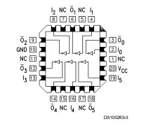 Specifications
If Military/Aerospace specified devices are required,please contact the National Semiconductor Sales ffice/Distributors for availability and specifications.
Supply Voltage (VCC) ....................................−0.5V to +7.0V
DC Input Diode Current (IIK)
VI = −0.5V ................................................................−20 mA
VI = VCC + 0.5V ........................................................+20 mA
DC Input Voltage (VI) ...........................−0.5V to VCC + 0.5V
DC Output Diode Current (IOK)
VO = −0.5V ...............................................................−20 mA
VO = VCC + 0.5V .......................................................+20 mA
DC Output Voltage (VO) ........................−0.5V to VCC + 0.5V
DC Output Source
or Sink Current (IO) ..................................................±50 mA
DC VCC or Ground Current
per Output Pin (ICC or IGND) .....................................±50 mA
Storage Temperature (TSTG) .......................−65 to +150
Junction Temperature (TJ)
CDIP ............................................................................175
Supply Voltage (VCC)'AC ...................................2.0V to 6.0V
Input Voltage (VI) ................................................0V to VCC
Output Voltage (VO) ............................................0V to VCC
Operating Temperature (TA)
54AC .........................................................−55 to +125
Note 1: Absolute maximum ratings are those values beyond which damage to the device may occur. The databook specifications should be met, without exception, to ensure that the system design is reliable over its power supply, temperature, and output/input loading variables. National does not recommend operation of FACT™ circuits outside databook specifications.
| Temperature Min |
-55 deg C |
| Temperature Max |
125 deg C |
| View Using Catalog |
DescriptionThe 54AC14 contains six inverter gates each with a Schmitt trigger input. The 54AC14 contains six logic inverters which accept standard CMOS input signals and provide standard CMOS output levels. They are capable of transforming slowly changing input signals into sharply defined, jitter-free output signals. In addition, they have a greater noise margin than conventional inverters.
The 54AC14 has hysteresis between the positive-going and negative-going input thresholds (typically 1.0V) which is determined internally by transistor ratios and is essentially insensitive to temperature and supply voltage variations.
The 54AC14 contains six inverter gates each with a Schmitt trigger input. The 54AC14 contains six logic inverters which accept standard CMOS input signals and provide standard CMOS output levels. They are capable of transforming slowly changing input signals into sharply defined, jitter-free output signals. In addition, they have a greater noise margin than conventional inverters.
The 54AC14 has hysteresis between the positive-going and negative-going input thresholds (typically 1.0V) which is determined internally by transistor ratios and is essentially insensitive to temperature and supply voltage variations.
Application Notes
| Title |
Size in Kbytes |
Date |
|
| AN-927: Total Dose Testing of Advanced CMOS Logic at Low Voltage |
109 Kbytes |
5-Jan-96 |
Download |
If you have trouble printing or viewing PDF file(s), see Printing Problems.
|
More Application Notes
| Title |
Size in Kbytes |
Date |
|
| AN-925: Radiation Design Test Data for Advanced CMOS Product |
194 Kbytes |
5-Aug-95 |
Download |
If you have trouble printing or viewing PDF file(s), see Printing Problems.
|

 54AC14 Data Sheet