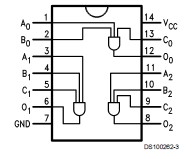
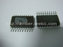
Features: ` ICC reduced by 50%` Outputs source/sink 24 mA` Standard Military Drawing (SMD)` 'AC11: 5962-87611PinoutSpecifications Temperature Min -55 deg C Temperature Max 125 deg C View Using CatalogIf Military/Aerospace specified devices are required,please contact the National Semi...
54AC11: Features: ` ICC reduced by 50%` Outputs source/sink 24 mA` Standard Military Drawing (SMD)` 'AC11: 5962-87611PinoutSpecifications Temperature Min -55 deg C Temperature Max 125 deg C Vie...
SeekIC Buyer Protection PLUS - newly updated for 2013!
268 Transactions
All payment methods are secure and covered by SeekIC Buyer Protection PLUS.
` ICC reduced by 50%
` Outputs source/sink 24 mA
` Standard Military Drawing (SMD)
` 'AC11: 5962-87611
Temperature Min | -55 deg C |
Temperature Max | 125 deg C |
View Using Catalog |
If Military/Aerospace specified devices are required,please contact the National Semiconductor Sales Office/Distributors for availability and specifications.
Supply Voltage (VCC) ...............................−0.5V to +7.0V
DC Input Diode Current (IIK)
VI = −0.5V ...........................................................−20 mA
VI = VCC + 0.5V ...................................................+20 mA
DC Input Voltage (VI) ......................−0.5V to VCC + 0.5V
DC Output Diode Current (IOK)
VO = −0.5V ..........................................................−20 mA
VO = VCC + 0.5V ..................................................+20 mA
DC Output Voltage (VO) ..................−0.5V to V CC + 0.5V
DC Output Source
or Sink Current (IO) .............................................±50 mA
DC VCC or Ground Current
per Output Pin (ICC or IGND) ................................±50 mA
Storage Temperature (TSTG) ..................−65 to +150
Junction Temperature (TJ)
CDIP ........................................................................175
Supply Voltage (VCC)
'AC 2.0V to 6.0V
Input Voltage (VI) 0V to VCC
Output Voltage (VO) 0V to VCC
Operating Temperature (TA)54AC ...........−55 to +125
Minimum Input Edge Rate (DV/Dt)'AC Devices
VIN from 30% to 70% of VCC
VCC @ 3.3V, 4.5V, 5.5V ....................................125 mV/ns
Note 1: Absolute maximum ratings are those values beyond which damage to the device may occur. The databook specifications should be met, without exception, to ensure that the system design is reliable over its power supply, temperature, and output/input loading variables. National does not recommend operation of FACT™ circuits outside databook specifications.
The 'AC11 contains three 3-input AND gates.
More Application Notes
Title | Size in Kbytes | Date | |
AN-925: Radiation Design Test Data for Advanced CMOS Product | 194 Kbytes | 5-Aug-95 | Download |
AN-927: Total Dose Testing of Advanced CMOS Logic at Low Voltage | 109 Kbytes | 5-Jan-96 | Download |
If you have trouble printing or viewing PDF file(s), see Printing Problems. |
The 'AC11 contains three 3-input AND gates 54AC11.