Features: • Single +3.3V ±0.3V power supply
• Industry-standard x16 pinout, timing, functions,
and package
• 12 row, 10 column addresses (4)
13 row, 9 column addresses (8)
• High-performance CMOS silicon-gate process
• All inputs, outputs and clocks are LVTTL-compatible
• Extended Data-Out (EDO) PAGE MODE access
• 4,096-cycle CAS#-BEFORE-RAS# (CBR) REFRESH
distributed across 64ms
• Self refresh for low-power data retentionPinout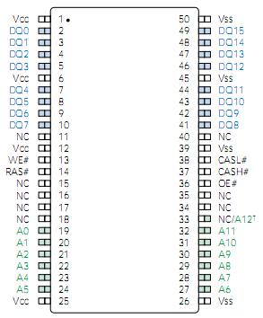 Specifications
Voltage on VCC Relative to VSS ..................-1V to +4.6V
Voltage on NC, Inputs or I/O Pins
Relative to VSS ....................................... -1V to +4.6V
Operating Temperature, TA (ambient)
Commercial .........................................0°C to +70°C
Extended (IT) ............................. -40°C to +85°C**
Storage Temperature (plastic) .........-55°C to +150°C
Power Dissipation ................................................... 1W
*Stresses greater than those listed under "Absolute Maximum Ratings" may cause permanent damage to the device. This is a stress rating only, and functional operation of the device at these or any other conditions above those indicated in the operational sections of this specification is not implied. Exposure to absolute maximum rating conditions for extended periods may affect reliability.
Description The 4 Meg x 16 DRAM MEM4X16E43VTW is a high-speed CMOS,dynamic random-access memory device containing 67,108,864 bits and designed to operate from 3V to 3.6V. The MEM4X16E43VTW is functionally organized as 4,194,304 locations containing 16 bits each. The 4,194,304 memory locations are arranged in 4,096 rows by 1,024 columns on the MEM4X16E43VTW. During READ or WRITE cycles, each location is uniquely addressed via the address bits: 12 row-address bits (A0-A11) and 10 column-address bits (A0-A9) on the MEM4X16E43VTW version. In addition, the byte and word accesses are supported via the two CAS# pins (CASL# and CASH#).
The CAS# functionality and timing related to address and control functions of MEM4X16E43VTW(e.g., latching column addresses or selecting CBR REFRESH) is such that the internal CAS# signal is determined by the first external CAS# signal (CASL# or CASH#) to transition LOW and the last to transition back HIGH. The CAS# functionality and timing related to driving or latching data is such that each CAS# signal independently controls the associated eight DQ pins.
The row address of MEM4X16E43VTW is latched by the RAS# signal, then the column address is latched by CAS#. This device provides EDO-PAGE-MODE operation, allowing for fast successive data operations (READ, WRITE or READ MODIFY-WRITE) within a given row.
The 4 Meg x 16 DRAM MEM4X16E43VTW must be refreshed periodi cally in order to retain stored data.

 4X16E43V Data Sheet


