42MX

Features: High Capacity• Single-Chip ASIC Alternative• 3,000 to 54,000 System Gates• Up to 2.5 kbits Configurable Dual-Port SRAM• Fast Wide-Decode Circuitry• Up to 202 User-Programmable I/O Pins High Performance• 5.6 ns Clock-to-Out• 250 MHz Performance...

product image

42MX Picture
SeekIC No. : 004230716 Detail

42MX: Features: High Capacity• Single-Chip ASIC Alternative• 3,000 to 54,000 System Gates• Up to 2.5 kbits Configurable Dual-Port SRAM• Fast Wide-Decode Circuitry• Up to 202 ...

floor Price/Ceiling Price

Part Number:
42MX
Supply Ability:
5000

Price Break

  • Qty
  • 1~5000
  • Unit Price
  • Negotiable
  • Processing time
  • 15 Days
Total Cost: $ 0.00

SeekIC Buyer Protection PLUS - newly updated for 2013!

  • Escrow Protection.
  • Guaranteed refunds.
  • Secure payments.
  • Learn more >>

Month Sales

268 Transactions

Rating

evaluate  (4.8 stars)

Upload time: 2024/11/23

Payment Methods

All payment methods are secure and covered by SeekIC Buyer Protection PLUS.

Notice: When you place an order, your payment is made to SeekIC and not to your seller. SeekIC only pays the seller after confirming you have received your order. We will also never share your payment details with your seller.
Product Details

Description


Features:

High Capacity
• Single-Chip ASIC Alternative
• 3,000 to 54,000 System Gates
• Up to 2.5 kbits Configurable Dual-Port SRAM
• Fast Wide-Decode Circuitry
• Up to 202 User-Programmable I/O Pins
High Performance
• 5.6 ns Clock-to-Out
• 250 MHz Performance
• 5 ns Dual-Port SRAM Access
• 100 MHz FIFOs
• 7.5 ns 35-Bit Address Decode HiRel Features
• Commercial, Industrial, and Military Temperature Plastic Packages
• Commercial, Military Temperature and MIL-STD-883
   Ceramic Packages
• QML Certification
• Ceramic Devices Available to DSCC SMD
Ease of Integration
• Mixed Voltage Operation (5.0V or 3.3V I/O)
• Synthesis-Friendly Architecture to Support ASIC Design
   Methodologies
• Up to 100% Resource Utilization and 100% Pin Fixing
• Deterministic, User-Controllable Timing
• Unique In-System Diagnostic and Verification Capability
   with Silicon Explorer II
• Low Power Consumption
• IEEE Standard 1149.1 (JTAG) Boundary Scan Testing
• 5.0V and 3.3V Programmable PCI-Compliant I/O


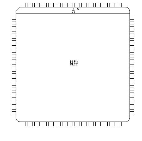
Pinout

  Connection Diagram


Specifications

Symbol Parameter Limits Units
VCCA
VCCI
DC Supply Voltage 0.5 to +7.0 v
VI Input Voltage 0.5 to VCC +0.5 v
VO Output Voltage 0.5 to VCC +0.5 v
TSTG Storage Temperature 65 to +150 °C
Notes:
1. Stresses beyond those listed under "Absolute Maximum
Ratings" may cause permanent damage to the device.
Exposure to absolute maximum rated conditions for extended
periods may affect device reliability. Devices should not be
operated outside the Recommended Operating Conditions.
2. Device inputs are normally high impedance and draw
extremely low current. However, when input voltage is greater
than VCCA + 0.5V or less than GND 0.5V, the internal
protection diode will be forward-biased and can draw
excessive current


Customers Who Bought This Item Also Bought

Margin,quality,low-cost products with low minimum orders. Secure your online payments with SeekIC Buyer Protection.
Cables, Wires - Management
Transformers
LED Products
Test Equipment
Programmers, Development Systems
Batteries, Chargers, Holders
View more