3D3215

Features: · All-silicon, low-power 3.3V CMOS technology· Vapor phase, IR and wave solderable· Auto-insertable (DIP pkg.)· Low ground bounce noise· Leading- and trailing-edge accuracy· Delay range: 1.5ns through 300ns· Total delay tolerance: 2% or 0.5ns (3.3V, 25C)· Temperature stability: ±1% typic...

product image

3D3215 Picture
SeekIC No. : 004229734 Detail

3D3215: Features: · All-silicon, low-power 3.3V CMOS technology· Vapor phase, IR and wave solderable· Auto-insertable (DIP pkg.)· Low ground bounce noise· Leading- and trailing-edge accuracy· Delay range: 1...

floor Price/Ceiling Price

Part Number:
3D3215
Supply Ability:
5000

Price Break

  • Qty
  • 1~5000
  • Unit Price
  • Negotiable
  • Processing time
  • 15 Days
Total Cost: $ 0.00

SeekIC Buyer Protection PLUS - newly updated for 2013!

  • Escrow Protection.
  • Guaranteed refunds.
  • Secure payments.
  • Learn more >>

Month Sales

268 Transactions

Rating

evaluate  (4.8 stars)

Upload time: 2024/11/20

Payment Methods

All payment methods are secure and covered by SeekIC Buyer Protection PLUS.

Notice: When you place an order, your payment is made to SeekIC and not to your seller. SeekIC only pays the seller after confirming you have received your order. We will also never share your payment details with your seller.
Product Details

Description


Features:

· All-silicon, low-power 3.3V CMOS technology
· Vapor phase, IR and wave solderable
· Auto-insertable (DIP pkg.)
· Low ground bounce noise
· Leading- and trailing-edge accuracy
· Delay range: 1.5ns through 300ns
· Total delay tolerance: 2% or 0.5ns (3.3V, 25C)
· Temperature stability: ±1% typical (0C-70C)
· Vdd stability: ±1% typical (3.0V-3.6V)
· Static Idd: 1.3ma typical
· Minimum input pulse width: 25% of total delay


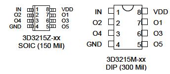
Pinout

  Connection Diagram

PIN DESCRIPTIONS
IN                  Delay Line Input
O1                 Tap 1 Output (20%)
O2                 Tap 2 Output (40%)
O3                 Tap 3 Output (60%)
O4                 Tap 4 Output (80%)
O5                 Tap 5 Output (100%)
VDD               +3.3 Volts
GND               Ground
N/C                 No Connection


Specifications

PARAMETER SYMBOL MIN MAX UNITS NOTES
DC Supply Voltage VDD -0.3 7.0 V  
Input Pin Voltage VIN -0.3 VDD+0.3 V  
Input Pin Current IIN -1.0 1.0 mA 25C
Storage Temperature TSTRG -55 150 C 10 sec
Lead Temperature TLEAD   300 C  


Description

The 3D3215 five-tap delay line architecture is shown in Figure 1. The delay line is composed of a number of delay cells connected in series.Each delay cell produces at its output a replica of the signal present at its input, shifted in time. The delay cells are matched and share the same compensation signals, which minimizes tap-to-tap delay deviations over temperature and supply voltage variations.


Customers Who Bought This Item Also Bought

Margin,quality,low-cost products with low minimum orders. Secure your online payments with SeekIC Buyer Protection.
Computers, Office - Components, Accessories
Line Protection, Backups
Integrated Circuits (ICs)
Circuit Protection
Memory Cards, Modules
View more