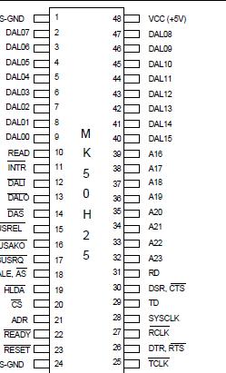
Features: ·System clock rate up to 33 MHz (MK50H25 - 33), 25 MHz (MK50H25 - 25), or 16 MHz (MK50H25 - 16).
·Data rate up to 20 Mbps continuous (MK50H25 - 33) or up to 51 Mbps bursted
·On chip DMA control with programmable burst length.
·DMA transfer rate of up to 13.3 Mbytes/sec using optional 5 SYSCLK DMA cycle (150 nS) at 33 MHz SYSCLK.
·Complete Level 2 implementation compatible with X.25 LAPB, ISDN LAPD, X.32, and X.75 Protocols.
·Handles all error recovery, sequencing, and S and U frame control.
·Pin-for-pin and architecturally compatible with MK5025 (X.25/LAPD), MK5027 (CCS#7) and MK5029(SDLC).
·Buffer Management includes:
- Initialization Block
- Separate Receive and Transmit Rings
- Variable Descriptor Ring and Window Sizes.
·Separate 64-byte Transmit and Receive FIFO.
·Programmable Transmit FIFO hold-off watermark.
·Handles all HDLC frame formatting:
- Zero bit insertion and deletion
- FCS (CRC) generation and detection
- Frame delimiting with flags
·Programmable Single or Extended Address and Control fields.
·Five programmable timer/counters: T1, T3, TP, N1, N2
·Programmable minimum frame spacing on transmission (number of flags between frames).
- Programmable from 1 to 62 flags between frames
·Selectable FCS (CRC) of 16 or 32 bits, and passing of entire FCS to buffer.
·Testing Facilities:
- Internal Loopback
- Silent Loopback
- Optional Internal Data Clock Generation
- Self Test.
·Programmable for full or half duplex operation
·Programmable Watchdog Timers for RCLK and TCLK (to detect absence of data clocks)
·Option causing received data to effectively be odd-byte aligned, in addition to standard evenbyte alignment.
·Available in 52 pin PLCC, 84 pin PLCC(for use with external ROM), or 48 pin DIP packages.
Pinout Specifications
| Symbol |
Parameter |
Value |
Unit |
| TUB |
Temperature Under Bias |
-25 to +100 |
|
| Tstg |
Storage Temperature |
-65 to +150 |
|
| VG |
Voltage on any pin with respect to ground |
-0.5 to VCC+0.5 |
V |
| Ptot |
Power Dissipation |
0.5 |
W |
Stresses above those listed under "Absolute Maximum Rating" may cause permanent damage to the above device.This is a stress rating only and functional operation of the device at these or any other condition above those ndicated in the operational sections of this specification is not implied. Exposure to absolute maximum rating onditions for extended periods may affect device reliability.
DescriptionThe SGS - Thomson 37956 Link Level Controller is a VLSI semiconductor device which provides complete link level data communications control conforming to the 1984 and 1988 CCITT versions of X.25. The MK50H25 will perform frame formating including: frame delimiting with flags, transparency (so-called "bit-stuffing"), error recovery by retransmission, sequence number control, S (supervisory) and U (unnumbered) frame control, plus FCS (CRC) generation and detection. The MK50H25 also supports X.75 and X.32 (with its XID frame support), as well as single channel ISDN LAPD (with its support of UI frames and extended addressing capabilities).
For added flexibility a transparent mode provides an HDLC transport mechanism without link layer support. This flexible transparent mode may be easily entered and exited without affecting the X.25 link status or the link state variables kept by the MK50H25. In this mode no protocol processing is done and it is up to the user to take care of the upper level software. Single or extended Address field filtering and Control field handling are optionally supported within the transparent mode.
One of the outstanding features of the 37956 is its buffer management which includes on-chip dual channel DMA. This feature allows users to receive and transmit multiple data frames at a time. (A conventional serial communications control chip plus a separate DMA chip would handle data for only a single block at a time.) The MK50H25 will move multiple blocks of receive and transmit data directly into and out of memory through the Host's bus. A possible system configuration for the MK50H25 is shown in figure 1.
The 37956 may be used with any of several popular 16 and 8 bit microprocessors, such as 68020, 68000, 6800, Z8000, Z80, 8086, 8088,80186, 80286, 80386SX, etc.
The 37956 may be operated in either full or half duplex mode. In half duplex mode, the RTS and CTS modem control pins are provided. In full duplex mode, these pins become user programmable I/O pins. All signal pins on the MK50H25 are TTL compatible. This has the advantage of making the MK50H25 independent of the physical interface. As shown in figure 1, line drivers and receivers are used for electrical connection to the physical layer.

 37956 Data Sheet


