Series: -
FET Type: MOSFET N-Channel, Metal Oxide
Transistor Type: -
Current - Collector (Ic) (Max): -
Voltage - Collector Emitter Breakdown (Max): -
Vce Saturation (Max) @ Ib, Ic: -
Current - Collector Cutoff (Max): -
DC Current Gain (hFE) (Min) @ Ic, Vce: -
Frequency - Transition: -
FET Feature: Standard
Drain to Source Voltage (Vdss): 500V
Packaging: Tube
Mounting Type: Through Hole
Current - Continuous Drain (Id) @ 25° C: 15A
Gate Charge (Qg) @ Vgs: 58nC @ 10V
Power - Max: 150W
Vgs(th) (Max) @ Id: 4V @ 1mA
Input Capacitance (Ciss) @ Vds: 2600pF @ 10V
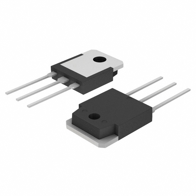
Package / Case: TO-3P-3, SC-65-3
Manufacturer: Toshiba
Supplier Device Package: TO-3P(N)
Rds On (Max) @ Id, Vgs: 490 mOhm @ 7A, 10V
DescriptionThe 2SK3314 is a kind of TOSHIBA field effect transistor which is desiged for the high speed, high current switching applications and switching regulator, DC to DC converter and motor drive applications.Features of 2SK3314 are:(1)low drain-source ON resistance: RDS(ON) is 0.35 ohms typ; (2)high forward transfer admittance: Yfs is 9.9 S typ; (3)enhancement-mode: Vth is 2.0 V to 4.0 V(VDS is 10 V and ID is 1 mA); (4)low leakage current: IDSS is 100 uA max when VDS is 500 V.
The absolute maximum ratings of 2SK3314 can be summerized as:(1): drain-source voltage, VDSS is 500 V; (2): drain-gate voltage(RGS is 20 kohms), VDGR is 500 V; (3): gate-source voltage, VGSS is ±30 V; (4): DC drain current, ID is 15 A; (5): drain power dissipation(ta is 25), PD is 150 W; (6): single pulse avalanche ennergy, EAS is 630 mJ; (7): avalanche current, IAR is 15 A; (8): repetitive avalanche energy, EAR is 15 mJ; (9): channel temperature, Tch is 150; (10): storage temeprature range, tstg is -55 to 150.
The electrical characteristics of 2SK3314 can be summerized as:(1): gate leakage current, IGSS is ±10 A max when VGS is ±25 V and VDS is 0 V; (2): drain-source breakdown voltage, V(BR)DSS is 500 V min when IG is 10 mA and VGS is 0 V; (3): drain cut-off current, IDSS is 100 uA max when VDS is 500 A and VGS is 0 V; (4): input capacitance, Ciss is 2600 pF typ when VDS is 10 V , VGS is 0 V and f is 1 MHz; (5): gate threshold voltage, Vth is 2.0 V min and 4.0 V max when VDS is 10 V and ID is 1 mA; (6): drain-source ON resistance, RDS(ON) is 0.35 ohm typ and 0.49 ohm max when VGS is 10 V and ID is 7 A.

 2SK3314 Data Sheet


