DescriptionThe 2SJ516 is a kind of P-channel MOS field effect transistor.It can be used for high speed,high current switching and chopper regulator,DC-DC converter and motor drive applications.It has some features as follows.(1) low drain-source on-resistance; (2)high forward transfer admittance; ...
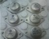
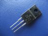
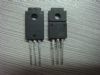
2SJ516: DescriptionThe 2SJ516 is a kind of P-channel MOS field effect transistor.It can be used for high speed,high current switching and chopper regulator,DC-DC converter and motor drive applications.It ha...
SeekIC Buyer Protection PLUS - newly updated for 2013!
268 Transactions
All payment methods are secure and covered by SeekIC Buyer Protection PLUS.
The 2SJ516 is a kind of P-channel MOS field effect transistor.It can be used for high speed,high current switching and chopper regulator,DC-DC converter and motor drive applications.It has some features as follows.(1) low drain-source on-resistance; (2)high forward transfer admittance; (3) low leakage current; (4) enhancement-mode.
The following is absolute maximum ratings of 2SJ516 at TA is 25. (1): drain-source voltage(VDSS) is -250 V; (2): gate-source voltage(VGSS) is ±20 V; (3): drain-gate voltage(VDGR) is -250 V; (4): DC drain current(ID) is -6.5 A and pulse drain current is -13 A; (5): drain power dissipation(PD) is 35 W ; (6): single pulse avalanche energy(EAS) is 157 mJ; (7): avalanche current(IAR) is -6.5 A; (8): repetitive avalanche energy(EAR) is 3.5 mJ; (9): channel temperature (TCH) is 150; (10): storage temperature range is from -55 to 150.
What comes next is the electrical characters of 2SJ516 at TA is 25. (1): the maximum gate leakage current is ±10 A when VDS is 0 and VGS is ±16 V; (2): the minimum drain-source breakdown voltage is -250 V at ID is -10 mA and VGS is 0 V; (3): the minimum gate threshold voltage is -1.5 V and is -3.5 V for the maximum at VDS is -10 V and ID is -1 mA; (4): the typical input capacitance is 1120 pF,the reverse transfer capacitance is 110 pF and the output capacitance is 320 pF when VDS is -10 V,VGS is 0 V and f is 1 MHz; (5): the typical gate-source charge is 19 nC and gate-drain charge is 10 nC when VDD is -200 V,VGS is -24 V and ID is -6.5 A; (6): the typical rise time is 17 ns,turn-on time is 34 ns,fall time is 6 ns and turn-off time is 71 ns.