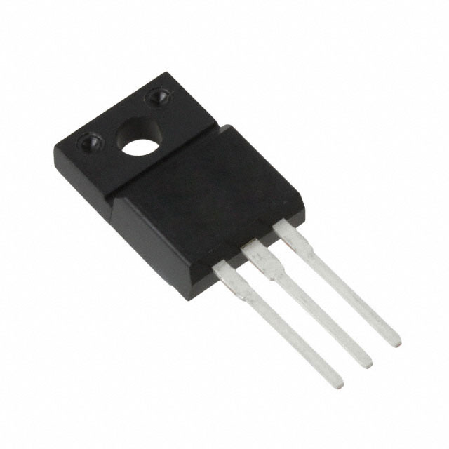
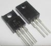
Features: SpecificationsDescription 2SJ319(L) is a kind of silicon P channel MOS FET high speed power switching. And it has five unique features: The first one is low on-resistance. The second one is high speed switching. The third one is low drive current . The forth one is no secondary breakdown. The fifth one is it is suitable for switching regulator , DC-DC converter.
There are some absolute maximum ratings about 2SJ319(L). Drain to source voltage(VDSS) is -200 V. Gate to souce voltage (VGSS) is ±20 V. Drain current (ID) is -3A. Drain peak current(ID(pulse)) is -12A. Body to drain diode reverse drain current(IDR) is -3A. Channel dissipation(Pch) is 20W.Channel temperature(Tch) is 150. Storage temperature(Tstg) is -55 to +150. Otherwise, there are also some electrical characterostocs about it. Drain to source breakdown voltage(V(BR)DSS ) is -200 V min when ID is -10 mA and VGS is 0. Gate to source breakdown voltage(V(BR)GSS) is ±20V min when IG is ±100 A and VGs is 0.Gate to source leak current (IGSS) is ±10 A max when VGS is±16 V, VDS is 0.Zero gate voltage drain current(IDSS) is100 A max when VDS is160 V, VGS is 0.Gate to source cutoff voltage (VGS (off) ) is2.0 V min and4.0 V max when ID is 1 mA, VDS is 10 V.Static drain to source on state resistance (RDS (on)) is 1.7min and 2.3 typ when ID is2 A, VGS is10 V .Forward transfer admittance (|yfs|) is 1.0 S min and 1.7 S when ID is 2 A, VDS is 10 V.Input capacitance(Ciss)is 330 pF typ when VDS is 10 V, VGS is 0 and f is 1 MHz.Output capacitance (Coss) is 130pF typ when VDS is 10 V, VGS is 0 and f is 1 MHz.Reverse transfer capacitance (Crss) is 25pF typ when VDS is 10 V, VGS is 0 and f is 1 MHz.Turn-on delay time (td (on) ) is 10 ns when ID is 2 A, VGS is 10 V and RL is 15 .Rise time (tr) is 30 ns when ID is 2 A, VGS is 10 V and RL is 15 .Turn-off delay time (td (off) ) is 40 ns when ID is 2 A, VGS is 10 V and RL is 15 . Fall time ( tf) is 30 ns when ID is 2 A, VGS is 10 V and RL is 15 .Body to drain diode forward voltage VDF( tf) is 1.15 V typ when IF is 3 A, VGS is 0.Body to drain diode reverse recovery time ( trr) is 180 ns when IF is 3 A, VGS is 0, and diF/dt is 50 A/s.
In a word , this is just a simple introduction of this kind of product, and if you are interested in it or you want to know detailed information about i2SJ319(L), please come to know more about our web. Thanks for your concern of our infomation!

 2SJ319(L) Data Sheet