DescriptionThe 2SD2584 is designed as toshiba transistor silicon NPN triple diffused type for hammer drive, pulse motor drive applications and high power switching applications.2SD2584 has two features. (1)It has low saturation voltage which would be max 1.5V at Ic=3A. (2)It has high DC current ga...
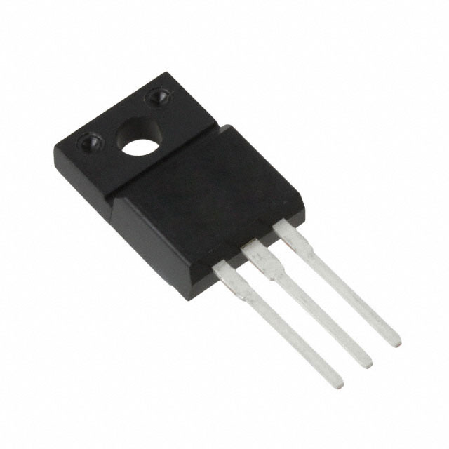
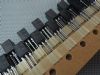
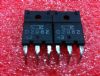
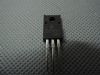
2SD2584: DescriptionThe 2SD2584 is designed as toshiba transistor silicon NPN triple diffused type for hammer drive, pulse motor drive applications and high power switching applications.2SD2584 has two featu...
SeekIC Buyer Protection PLUS - newly updated for 2013!
268 Transactions
All payment methods are secure and covered by SeekIC Buyer Protection PLUS.
The 2SD2584 is designed as toshiba transistor silicon NPN triple diffused type for hammer drive, pulse motor drive applications and high power switching applications.
2SD2584 has two features. (1)It has low saturation voltage which would be max 1.5V at Ic=3A. (2)It has high DC current gain which would be min 2000 at Vce=3V and Ic=3A. Those are all the main features.
Some absolute maximum ratings of 2SD2584 have been concluded into several points as follow. (1)Its collector to base voltage would be 120V. (2)Its collector to emitter voltage would be 100V. (3)Its emitter to base voltage would be 6V. (4)Its collector current would be 7A for DC and would be 10A for pulse. (5)Its base current would be 0.7A. (6)Its collector power dissipation would be 1.5W at Ta=25°C and it would be 20W at Tc=25°C. (7)Its junction temperature would be 150°C. (8)Its storage temperature range would be from -55°C to 150°C. It should be noted that stresses above those listed in absolute maximum ratings may cause permanent damage to device.
Also some electrical characteristics of 2SD2584 are concluded as follow. (1)Its collector cutoff current would be max 100uA. (2)Its emitter cutoff current would be min 0.75mA and max 3.0mA. (3)Its collector to emitter breakdown voltage would be min 100V. (4)Its DC current gain would be min 2000 and max 15000 with conditions of Vce=3V and Ic=3A and it would be min 1000 with conditions of Vce=3V and Ic=6A. (5)Its collector to emitter saturation voltage would be typ 0.9V and max 1.5V. (6)Its base to emitter saturation voltage would be typ 1.5V and max 2.0V. (7)Its switching time would be typ 0.5us for turn-on time and would be typ 6.0us for storage time and would be typ 1.0us for fall time.
It should be noted that the information contained herein is presented only as a guide for the applications of toshiba products. No responsibility is assumed by toshiba sorporation for any infringements of implication or otherwise under any intellectual property or other rights of toshiba corporation or others. And so on. If you have any question or suggestion or want to know more information please contact us for details. Thank you!