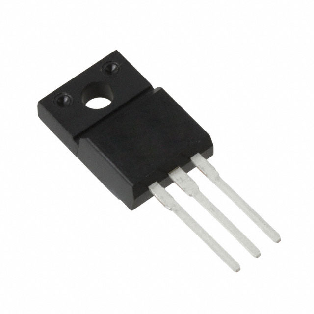
DescriptionThe 2SD201 is a silicon NPN power transistor with TO-3 package,large current capability,wide area of safe operation.The 2SD201 can be applied to for power amplifier and switching applications.The absolute maximun ratings of the 2SD201 at Ta=25°C having Collector-base Voltage VCBO is 90V...
2SD201: DescriptionThe 2SD201 is a silicon NPN power transistor with TO-3 package,large current capability,wide area of safe operation.The 2SD201 can be applied to for power amplifier and switching applicat...
SeekIC Buyer Protection PLUS - newly updated for 2013!
268 Transactions
All payment methods are secure and covered by SeekIC Buyer Protection PLUS.
The 2SD201 is a silicon NPN power transistor with TO-3 package,large current capability,wide area of safe operation.The 2SD201 can be applied to for power amplifier and switching applications.
The absolute maximun ratings of the 2SD201 at Ta=25°C having Collector-base Voltage VCBO is 90V;Collector-emitter Voltage VCEO is 60 V;Emitter-base Voltage VEBO is 6 V;Collector Current IC is 6A;Junction temperature is +150°C maximum;Storage temperature is -55 to +150°C ;collector power Dissipation(Tc=25°C) is 50W etc.
The 2SD201 provides fixed Erase and Program times, independent of the number of erase/program cycles that have occurred. The external oscillator mode can also be used with the internal divider function enabled (pin RC and pin DD = SGND). Due to the presence of the divider the bridge frequency is half the external oscillator frequency. The commutation of the bridge is triggered by the falling edge of the EXTDR signal with respect to V-LVS.
The pinout of 2SD201 is described below, the integrated circuit U6803B requires a stabilized supply voltage (VS = 5 V 5%) to comply with its electrical characteristics. An external buffer capacitor of C = 100 nF is recommended. An integrated 14 V Zener diode between VS and ground protects the supply pin.The online help system displays online, context-sensitive help for the user. Designed for procedural and quick reference, each functional subsystem has its own context-sensitive help. This system also provides tutorials and links to FAQs and an Online Support Forum to aid the designer in getting started. The HY29F080s sector erase architecture allows any number of array sectors to be erased and re- programmed without affecting the data contents of other sectors. Device erasure is initiated by executing the Erase Command. This initiates an internal algorithm that automatically preprograms the array (if it is not already programmed) before executing the erase operation. During erase cycles, the device automatically times the erase pulse widths and verifies proper cell margin.
At present there is not too much information about this model.If you are willing to find more about 2SD201, please pay attention to our web! We will promptly update the relevant information.