Features: SpecificationsDescriptionThe 2N5463 is designed as low cost P-channel JFETs which provide all-around performance in a wide range of amplifier and analog, switch applications. It features two ranges of gate-source breakdown voltage, good gain, and low capacitance. Its P-channel constructi...
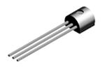
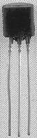
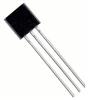
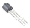
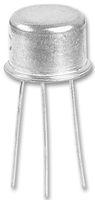
2N5463: Features: SpecificationsDescriptionThe 2N5463 is designed as low cost P-channel JFETs which provide all-around performance in a wide range of amplifier and analog, switch applications. It features t...
SeekIC Buyer Protection PLUS - newly updated for 2013!
268 Transactions
All payment methods are secure and covered by SeekIC Buyer Protection PLUS.
The 2N5463 is designed as low cost P-channel JFETs which provide all-around performance in a wide range of amplifier and analog, switch applications. It features two ranges of gate-source breakdown voltage, good gain, and low capacitance. Its P-channel construction also affords the designer simplicity for many applications. Its TP-92 package is compatible with a wide range of tape and reel options for automated assembly.
Some absolute maximum ratings of 2N5463 have been concluded into several points as follow. The first one is about its gate-drain voltage which would be 60V. The second one si about its gate to source voltage which would be 60V. The third one is about its gate current which would be 10mA. The fourth one is about its power dissipation which would be 310mW. The fifth one is about its power derating which would be 2.8mW/°C. The sixth one is about its operating junction temperature range which would be from -55°C to +135°C. The seventh one is about its storage temperature range which would be from -65°C to +150°C. The eighth one is about its lead temperature which would be 300°C.
And some electrical characteristics about 2N5463. The first one is about its gate-source breakdown voltage which would be min 60V. The second one is about its gate to source cutoff voltage which would be min 0.75V and max 6V. The third one is about its saturation drain current which would be min -1mA and max -5mA. The fourth one is about its gate reverse current which would be max 5nA. The fifth one is about its gate operating current which would be typ 3pA. The sixth one is about its drain cutoff current which would be -5pA. The seventh one is about its gate to source voltage which would be min 0.5V and max 4V. The eighth one is about its gate to source forward voltage which would be typ -0.7V. And so on. For more information please contact us.