Max Input Freq
:
Propagation Delay (Max)
:
Packaging
:
Number of Outputs
: 5
Maximum Operating Temperature
: + 70 C
Minimum Operating Temperature
: 0 C
Package / Case
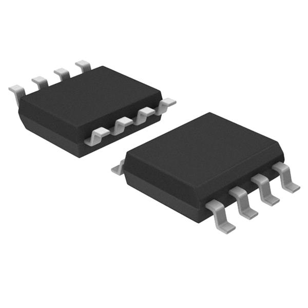
: SOIC-8
Supply Voltage - Max
: 3.6 V
Supply Voltage - Min
: 3 V
Maximum Power Dissipation
: 0.7 W
Specifications | Input Frequency | 10-133 MHz |
| No. of Inputs | 1 |
| Temperature | C |
| Output Frequency | 10-133 MHz |
| No. of Outputs | 5 |
| Voltage | 3.3 V |
| Package | SOIC 8 |
| Speed | NA |
| Input | 3.3 V LVTTL |
| Output | 3.3 V LVTTL |
| Output Skew | 0.25 ns |
| Max Prop Delay | 0.35 ns |
| Jitter cycle-to-cycle | 0.2 ns |
| Type | Zero Delay Buffer |
DescriptionHI SPD PHASE LOCK LOOP
The IDT2305 is a low phase noise, high-speed PLLbased, low-skew zero delay buffer. Based on the IDTproprietary low jitter Phase Locked Loop (PLL)techniques, the device provides four low skew outputs at speeds up to 133 MHz at 3.3 V. The outputs can be generated from the PLL (for zero delay), or directly from the input (for testing), and can be set to tri-state mode or to stop at a low level. The PLL feedback is on-chip and is obtained from the CLKOUT pad.
The IDT2305 is available in two different versions. The IDT2305-1 is the base part. The IDT2305-1H is a high drive version with faster rise and fall times.
Clock outputs from 10 to 133 MHz
Zero input-output delay
Four low skew (<250 ps) outputs
Device-to-device skew <700 ps
Full CMOS outputs with 25 mA output drive capability at TTL levels
5 V tolerant CLKIN
Tri-state mode for board-level testing
Advanced, low power, sub-micron CMOS process
Operating voltage of 3.3 V
Industrial temperature range available
Packaged in 8-pin SOIC
 2305-1DCG Data Sheet


