
Signal Processing
Index 95
PWM
Published:2009/7/20 23:54:00 Author:Jessie
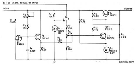
With S1 at 1, circuit is unjunction-transistor pulse generator with prf variable from 13 to 25 kc, and duty cycle variable from 0 to 100%. With S1 at 2, circuit is modulator whose output pulse width varies with level of external d-c signal.-D. L. Patillo, Pulse Generator Circuit Doubles Modulator, Electronics, 38:8, p 91-92. (View)
View full Circuit Diagram | Comments | Reading(968)
Voltage_controlled_sine_wave_oscillator
Published:2009/7/20 23:55:00 Author:Jessie

Voltage-controlled sine-wave oscillator. Two AD534 multipliers are used to form integrators with controllable time constants in a second-order differential-equation feedback loop. The waveform shows the VCO's response to a ramp input (courtesy Analog Devices, Inc.). (View)
View full Circuit Diagram | Comments | Reading(0)
100_KC_HYBRID_BALANCED_MODULATOR
Published:2009/7/21 0:09:00 Author:Jessie
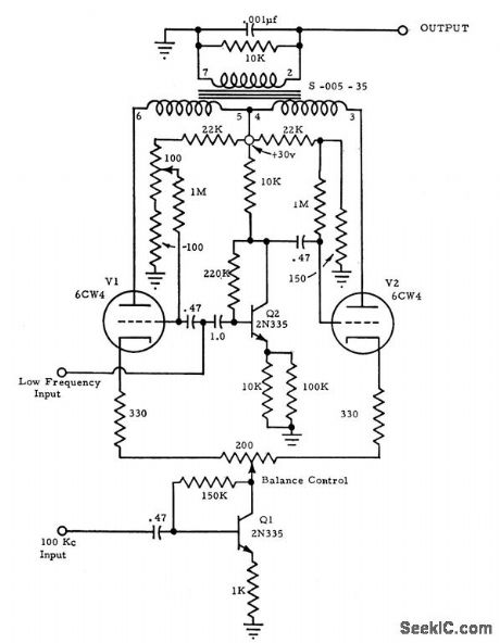
Circuit is essentially balanced bridge, with carrier injected by Q1. Balance is maintained by balance control and by bias adjustment on VI. Modulation is achieved by unbalancing bridge in accordance with low-frequency in.put signal, using phase inverter Q2 to make both tubes unbalance bridge in same direction.-J. Chirnitch, Hybrid Balanced Modulator for 100 Kc, EEE, 10:10, p 30. (View)
View full Circuit Diagram | Comments | Reading(1085)
TRANSFORMER_T_R_I_G_G_E_R_E_D_MAGNETRON_MODULATOR
Published:2009/7/21 0:10:00 Author:Jessie
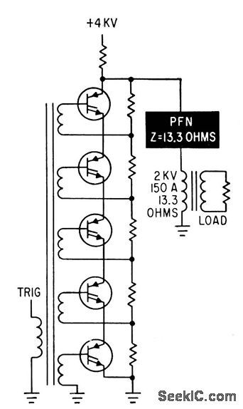
Success of circuit depends on availability of five pnpn transistors with breakover voltages of at least 800 v, in order to deliver 300-kw pulses to load through pulse-forming network PFN.-F. A. Gateka and M. L. Embree, Semiconductor Modulators for Modem Magnetrons, Electronics, 35:37, p 42-45. (View)
View full Circuit Diagram | Comments | Reading(606)
DISCRETE_SEQUENCE_OSCILLATOR
Published:2009/7/9 1:15:00 Author:May

The swept-frequency oscillator offers an inexpensive source of discrete frequencies for use in testing digital circuits. In this configuration, the circuit generates an 80-second sequence of eight frequencies, dwelling for 10 seconds on each frequency. You can change the dwell time or the number of frequencies.Frequencies can range from 0.005 Hz to 1 MHz.
The programmable crystal oscillators, PXOs, IC2 and IC4 can each generate 57 frequencies in response to an 8-bit external code. IC2 contains a 1-MHz crystal and produces a 0.05-Hz output. IC4 contains a 600-kHz crystal; its output changes in response to the combined outputs of the 12-stage binary counter IC3 (Q1 and Q2) and the PXO IC2.
To generate more frequencies, you can use one or more of IC3's outputs, (Q3, Q4, Q5) to drive one or more of IC4's inputs (P4, P5, P6). Similarly, you can rewire IC2 or drive it with other logic to control the duration of each frequency. IC1, a monostable multivibrator, provides a system reset. It initiates the sequence shown, beginning at 60 Hz, in response to a positive pulse. (View)
View full Circuit Diagram | Comments | Reading(720)
50DUTY_CYCLE_OSCILLATOR
Published:2009/7/9 1:34:00 Author:May


Frequency of oscillation depends on the R1/C1 time constant and allows frequency adjustment byvarylng R1. (View)
View full Circuit Diagram | Comments | Reading(732)
HCU_HCT_BASED_OSCILLATOR
Published:2009/7/9 1:33:00 Author:May


When frequency stability is not of prime importance, a simple, yet retable, digital clock oscillator can be made with the aid of relatively few components. High-speed CMOS (HCU/HCT) inverters or gates with an inverter function are eminently suitable to make such oscillators, thanks to their low power con-sumption, good output signal definition, and extensive frequency range.
The circuit as shown uses two inverters in a 74HCT04 or 74HCU04. The basic design equations are:
With RS and R calculated for a given frequency and value of C, both resistors can be realized as presets to enable precise setting of the output frequency and the duty factor. Do not forget, however, to fit small series resistors in series with the presets, in observance of the minimum values for R and RS as given in the design equations. The values quoted for IC are only valid if the inputs of the remaining gates are g fillnded.
(View)
View full Circuit Diagram | Comments | Reading(1302)
2_METER_RECEIVER_CALIBRATOR
Published:2009/7/21 2:08:00 Author:Jessie
Checks both frequency and sensitivity of amateur FM receiver Starts with 3-MHz crystal and provides markers every 30 kHz or every 300 kHz Energy levels are so low that only simple 100-ohm attenuator is needed. Article covers construction and calibration. CR9-CR12 are silicon rated 200 PIV at 500mA, such as HEP156 DS2 is 117-V neon T2 is 12V at 0.3A.-H.Lukoff.A 2-Meter Frequency and Sensitivity Calibrator,QST,Feb,1976,p34-36. (View)
View full Circuit Diagram | Comments | Reading(689)
TWIN_TEE_TONE_OSCILLATOR
Published:2009/7/21 2:09:00 Author:Jessie

A 2N2222 transistor is used in a twin-tee oscillator, followed by a FET buffer circuit. (View)
View full Circuit Diagram | Comments | Reading(1368)
UJT_OSCILLATOR
Published:2009/7/21 2:11:00 Author:Jessie

When power is connected to the circuit, C1 charges through R1 and R3. When the voltage reaches the UJT gate's (G) threshold voltage (usually around 0.5 to 0.8 of the supply voltage), the dynamic resistance between B2 and B1 drops to a very low value. Capacitor C1 then discharges through the emitter-base junction and the 8-Ω speaker. The frequency of the UJT oscillator is determined by the values of C1, R1, and R3. (View)
View full Circuit Diagram | Comments | Reading(816)
NE602_HARTLEY_VFO_CIRCUIT
Published:2009/7/21 2:12:00 Author:Jessie

In this circuit, L1 is tapped at about one-third to one-fourth from the ground end. L1 is about 10/f MHz, while C1 is chosen to resonate L1 to the desired frequency. (View)
View full Circuit Diagram | Comments | Reading(1338)
WIDE_RANGE_OSCILLATOR
Published:2009/7/9 1:31:00 Author:May

The gain control allows the oscillator to maintain essentially constant output over its range. The circuit functions over 160 kHz to 12 MHz with essentially constant amplitude. (View)
View full Circuit Diagram | Comments | Reading(1629)
HARTLEY_OSCILLATOR
Published:2009/7/21 2:13:00 Author:Jessie

The oscillator's operating frequency is determined by the values of L1 and C3. The feedback level is determined by the location of the tap on L1, which normally will be about one-fifth to one-fourth of the total turns. As an example, the Hartley oscillator will operate in the 5-MHz range with the following LC values: L1 is 20 turns of 18 enameled copper wire close wound on a 1-inch plastic form with a tap up five turns from the bottom. Capacitor C3 can be any small variable capacitor with a maximum capacitance value of 100 pF. With the proper LC values, the Hartley oscillator can operate from audio to UHF. (View)
View full Circuit Diagram | Comments | Reading(0)
VOLTAGE_TUNED_HARTLEY_JFET_VFO
Published:2009/7/21 2:15:00 Author:Jessie

This voltage-tuned JFET Hartley oscillator can be made to sweep its entire frequency range by applying a sawtooth waveform that rises from 0 to 12 V to the Vt input. In this circuit, a varactor is used for the tuning element instead of an air-core inductor. The frequency range is around 5 MHz. (View)
View full Circuit Diagram | Comments | Reading(683)
VARIABLE_VNEN_BRIDGE_OSCILLATOR
Published:2009/7/9 1:30:00 Author:May


A Wien-bridge oscillator can be made variable by using two frequency-determining parts that are var-ied simultaneously at high tracking accuracy. High-quality tracking potentiometers or variable capacitors are, however, expensive and difficult to obtain. To avoid having to use such a component, this oscillator was designed to operate with a single potentiometer. The output frequency, f0,is calculated from:
With preset P2 you can adjust the overall amplification so that the output signal has a easonably stable amplitude, 3.5 VPP max., over the entire frequency range. The stated components allow the frequency to be adjusted between 350 Hz and 3.5 kHz. (View)
View full Circuit Diagram | Comments | Reading(1551)
MODIFIED_HARTLEY_OSCILLATOR
Published:2009/7/21 2:15:00 Author:Jessie

A. F. Lampkin, in 1939, showed that a high-C Hartley oscillator (as typically used in the once popular ECO VFO) could be improved by a factor of about 10 times simply by tapping the grid (gate or base) connection down the coil. (View)
View full Circuit Diagram | Comments | Reading(0)
NE602_HARTLEY_OSCILLATOR
Published:2009/7/21 2:16:00 Author:Jessie

In this Hartley VFO, feedback is provided via a tap on the inductor. (View)
View full Circuit Diagram | Comments | Reading(702)
HARTLEY_JFET_OSCILLATOR
Published:2009/7/21 2:19:00 Author:Jessie

This simple Hartley JFET oscillator has a built-in zener-diode regulator to condition the power-supply voltage down to 9.1 V. L1 depends on the desired frequency. Typical values are C1=5 to 50pF variable, C2=100 pF plus a 3-to 30-pF trimmer, and L1=14μH (for 3.5 MHz). L1 should be mechanically rigid, should have an air core (do not use ferrite cores because of drift effects), and should have Q ≥ 200 for best stability. The tap will be typically 10 to 25 percent of the total turns. (View)
View full Circuit Diagram | Comments | Reading(1330)
NE602_OSCILLATOR_CIRCUIT
Published:2009/7/21 2:28:00 Author:Jessie

If the LO signal of the NE602 is sent directly to the output pins, the device can be used as a low-cost, high-frequency oscillator. (View)
View full Circuit Diagram | Comments | Reading(1169)
STRIP_LINE_OSCILLATOR
Published:2009/7/21 2:48:00 Author:Jessie

The figure shows a prototype strip tine oscillator that is capable of providing an operating range of 3.5:1 before oscillation ceases Length A∶40 mm,width B∶2 mm,width C:1 mm To change the frequency range,alter the length A and the length of the output coupling wire Typical frequencies with C=0 pF are about 145 MHz;with 27 pF, about 80 MHz; with 56 pF, about 60 MHz;and with 150 pF, about 36 MHz (plate-ceramic capacitors). With 1/16-inch double-sided PC board, note that the bottom ground plane covers the whole of the board. The output is about 0 dBm. The U310 FET is pushed through from the bottom side of the PC board until it touches the ground plane and is soldered directly to the ground plane. (View)
View full Circuit Diagram | Comments | Reading(695)
| Pages:95/195 At 2081828384858687888990919293949596979899100Under 20 |
Circuit Categories
power supply circuit
Amplifier Circuit
Basic Circuit
LED and Light Circuit
Sensor Circuit
Signal Processing
Electrical Equipment Circuit
Control Circuit
Remote Control Circuit
A/D-D/A Converter Circuit
Audio Circuit
Measuring and Test Circuit
Communication Circuit
Computer-Related Circuit
555 Circuit
Automotive Circuit
Repairing Circuit