Oscillator Circuit
A_555_USED_AS_AN_RC_AUDIO_OSCILLATOR
Published:2009/7/6 21:57:00 Author:May | From:SeekIC


Circuit Notes
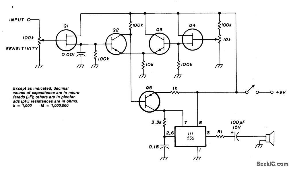
Transistor Q5 and the 1000 ohm resistor form the variable element needed for controlling the frequency of VDO by limiting the charging current flowing into the 0.15μF timing capacitor according to the forward bias being applied to Q5. As the voltage on pins 2 and 6 of U1 reach 2/3 VCC (about 6 volts with a 9-volt supply) the timer will fire and pin 3 will be pulled low. Pin 7, an open collector output, goes low and begins to discharge the timing capacitor-through the 3.3 kilohm resistor. The discharge time provided by this resistor assures a reasonable, although asymmetrical, waveform for the aural signal generated by U1. At 1/3 VCC the intemal flip-flop resets, the output on pin 3 goes high, the open collector output on pin 7 floats, and the timing cycle begins again.
Reprinted Url Of This Article:
http://www.seekic.com/circuit_diagram/Signal_Processing/Oscillator_Circuit/A_555_USED_AS_AN_RC_AUDIO_OSCILLATOR.html
Print this Page | Comments | Reading(3)

Article Categories
power supply circuit
Amplifier Circuit
Basic Circuit
LED and Light Circuit
Sensor Circuit
Signal Processing
Electrical Equipment Circuit
Control Circuit
Remote Control Circuit
A/D-D/A Converter Circuit
Audio Circuit
Measuring and Test Circuit
Communication Circuit
Computer-Related Circuit
555 Circuit
Automotive Circuit
Repairing Circuit
Code: