Remote Control Circuit
The time delay circuit diagram composed of transistor
Published:2011/9/13 1:51:00 Author:Rebekka | Keyword: transistor , time delay | From:SeekIC


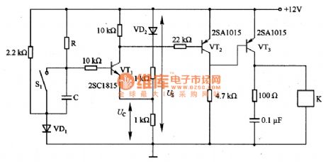
(a) Timedelay circuit
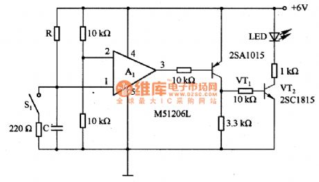
(b) Timedelay circuit
It can set delay time according to the voltage Us and resistor R. In the circuit, S1 is the the discharge switch of capacitor C. When the switch S1 is closed, the stored charge on C will be released through S1 to ensure the accuracy of the delay time the next time. VD1 and VD2 are used to eliminate the impact of VT1 by its voltage UBE. In the circuit, the load current can be only 5OnA. If VT3 is replaced by Darlington transistor, the load current will be increased. VT1 uses 2SC1815; VT2 and VT3 use 2SAlO15; VD1 and VD2 use 1S1588. Delay time T = RC1n1 / (1-K), K = Uc / Us. Figure 1 (b) is a time delay circuit composedof the transistor and the comparator. It is similar with the circuit shown in Figure 1(a). The comparison circuit uses comparator integrated chip M51206L. It is not effected by environmental temperature and supply voltage variations. Therefore, the circuit is very stable. If VT2 uses the Darlington power transistor, you can drive higher current load.
Reprinted Url Of This Article:
http://www.seekic.com/circuit_diagram/Remote_Control_Circuit/The_time_delay_circuit_diagram_composed_of_transistor.html
Print this Page | Comments | Reading(3)

Article Categories
power supply circuit
Amplifier Circuit
Basic Circuit
LED and Light Circuit
Sensor Circuit
Signal Processing
Electrical Equipment Circuit
Control Circuit
Remote Control Circuit
A/D-D/A Converter Circuit
Audio Circuit
Measuring and Test Circuit
Communication Circuit
Computer-Related Circuit
555 Circuit
Automotive Circuit
Repairing Circuit
Code: