power supply circuit
High_speed_15_A_MOSFET_drivers
Published:2009/7/23 23:24:00 Author:Jessie | From:SeekIC


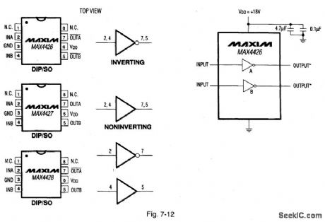
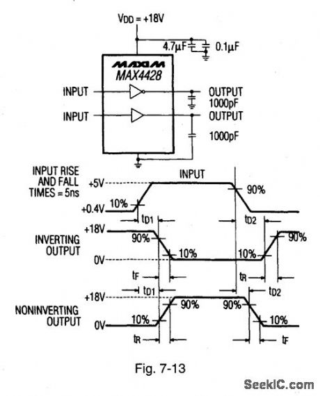
Figure 7-12 shows the basic connections for the MAX4426/27/28 drivers. Such ICs rapidly charge and discharge the gate capacitance of the largest MOSFETs to within millivolts of the supply. The typical on resistance is 4 Ω, the delay times are 10 ns for tD1 and 25 ns for tD2, the peak output current is 1.5 A, rise and fall times are typically 20 ns with 1000-pF loads, the operating range is 4.5 V to 18 V, and the power consumption is 1.8 mA with a logic-1 output and 200 μA with a logic-0 input. The ICs are TTL/CMOS compatible and will withstand greater than 500-mA reverse current. Figure 7-13 is a test circuit. Maxrvt HIGH-RELIABILITY DATA BOOK, 1993, P. 4-5, 4-6.
Reprinted Url Of This Article:
http://www.seekic.com/circuit_diagram/Power_Supply_Circuit/High_speed_15_A_MOSFET_drivers.html
Print this Page | Comments | Reading(3)

Article Categories
power supply circuit
Amplifier Circuit
Basic Circuit
LED and Light Circuit
Sensor Circuit
Signal Processing
Electrical Equipment Circuit
Control Circuit
Remote Control Circuit
A/D-D/A Converter Circuit
Audio Circuit
Measuring and Test Circuit
Communication Circuit
Computer-Related Circuit
555 Circuit
Automotive Circuit
Repairing Circuit
Code: