power supply circuit
Dc_stabilization_with_differential_input_and_a_gain_of_1000
Published:2009/7/24 20:54:00 Author:Jessie | From:SeekIC
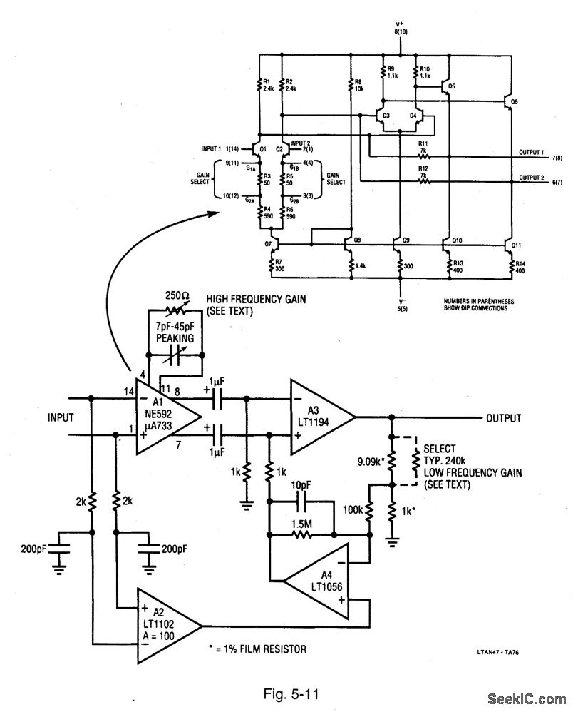
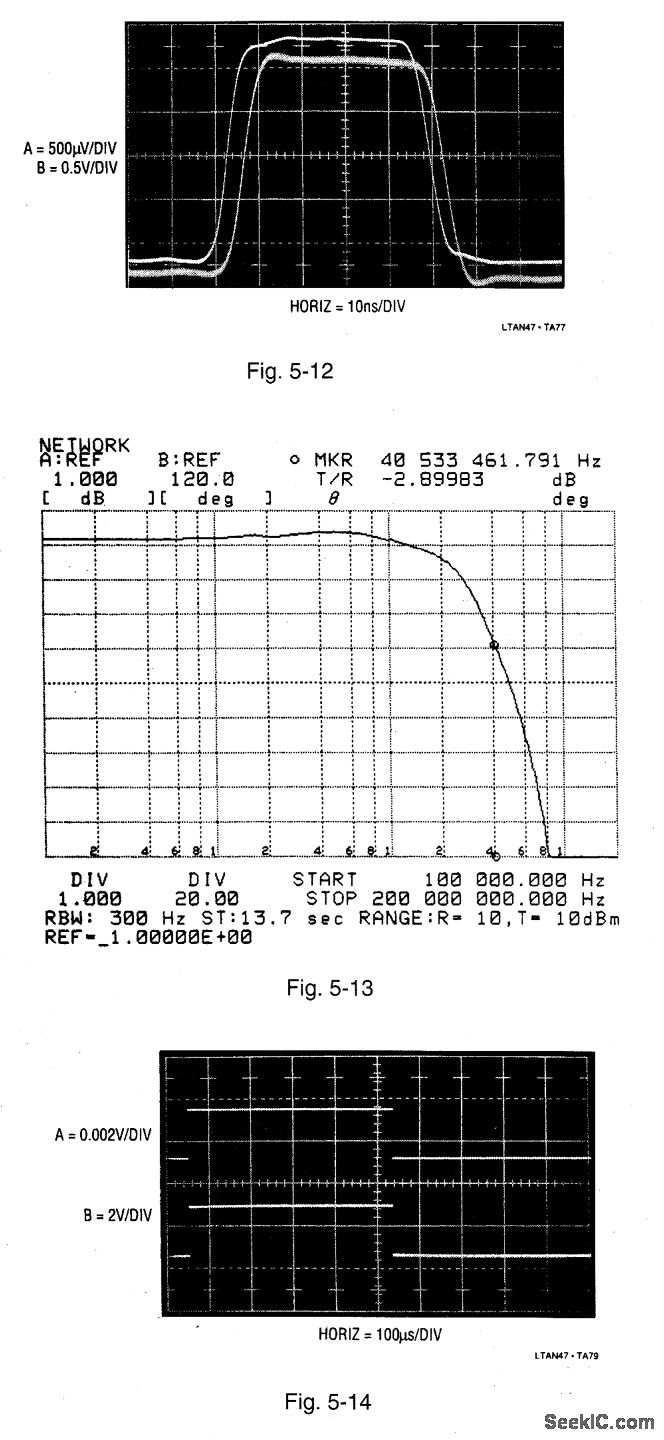
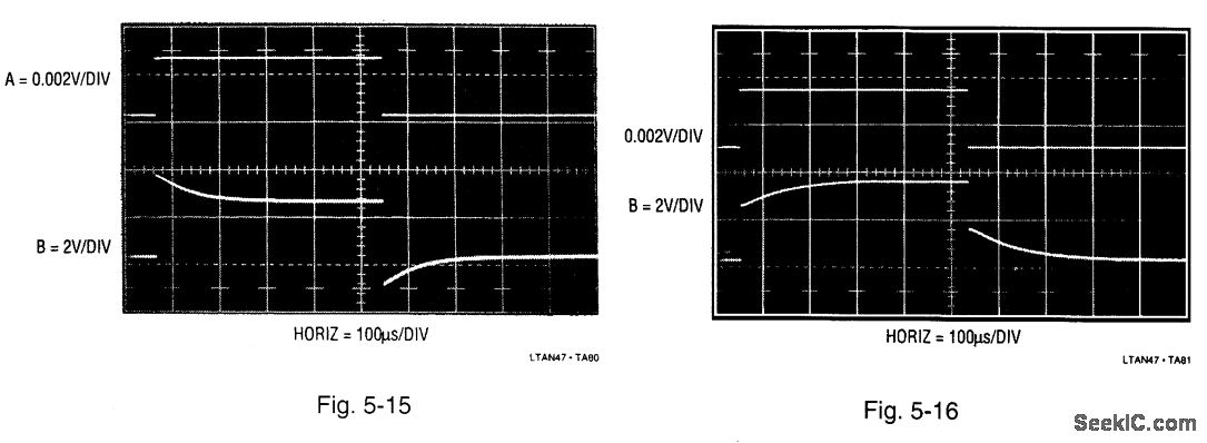
Figure 5-11 is similar to Fig. 5-9, but with a gain of 1000. The Fig. 5-11 circuit bandwidth is about 35 MHz, with full-power response available to 10 MHz. The rise time is 7 ns and delay is less than 7.5 ns. Input noise is about 15 μV broadband.Figure 5-12 shows the circuit response to a 60-ns, 2.5-mV pulse (trace A). The ×1000 output (trace B) has delay and rise times in the 5-ns to 7-ns range. Peaking can be trimmed with the adjustment at A1. Figure 5-13 plots the circuit gain versus frequency. Gain is flat within 0.5 dB to 20 MHz, with the -3-dB point at 38 MHz. The edge peaking shown in Fig. 5-12 shows up in Fig. 5-13 as a very slight gain increase, starting at about 1 MHz and continuing out to about 15 MHz. (This gain increase can be trimmed with the peaking adjustment, if necessary.) To use the circuit, apply a low-frequency or dc signal of known amplitude and adjust the low-frequency gain (parallel resistor) for a ×1000 output (after the output has settled). Next, adjust the high-frequency gain pot so that the output signal front and rear corners have amplitudes identical to the settled portion. Finally, trim the peaking-adjustment capacitor for best settling of the output pulse front and rear corners. Figure 5-14 shows the input (trace A) and output (trace B) waveforms with all adjustments properly set. Figure 5-15 shows the effects of too much ac gain (excessive peaking). figure 5-16 shows the effects of too much dc gain (long trailing response, with incorrect amplitude). LINEAR TECHNOLOGY, APPLICATION NOTE 47, P. 36, 37.
Reprinted Url Of This Article:
http://www.seekic.com/circuit_diagram/Power_Supply_Circuit/Dc_stabilization_with_differential_input_and_a_gain_of_1000.html
Print this Page | Comments | Reading(3)

Article Categories
power supply circuit
Amplifier Circuit
Basic Circuit
LED and Light Circuit
Sensor Circuit
Signal Processing
Electrical Equipment Circuit
Control Circuit
Remote Control Circuit
A/D-D/A Converter Circuit
Audio Circuit
Measuring and Test Circuit
Communication Circuit
Computer-Related Circuit
555 Circuit
Automotive Circuit
Repairing Circuit
Code: