Measuring and Test Circuit
The application circuit of the single chip wide frequency band phase difference test system AD8302
Published:2011/8/14 22:38:00 Author:qqtang | Keyword: application circuit, single chip, phase difference, test system | From:SeekIC
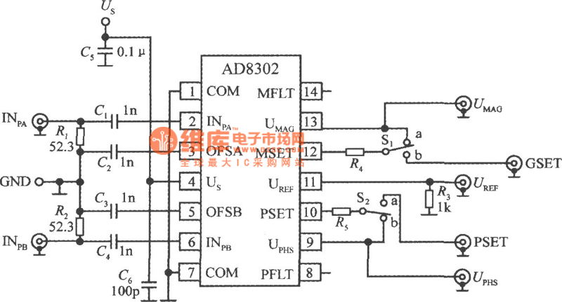
The AD8302 application circuit is shown in the figure. R1 and R2 are the input terminals. R3 is the load of the UREF output terminal. C1 and C4 are the AC input coupling capacitor, C2 and C3 are the filtering capacitors, C5 and C6 are the power supply decoupling capacitors. S1 is the gain test pattern/comparator pattern selecting switch, by pulling S2 to gear a, the phase difference test pattern; when it is pulled to gear b, the comparator pattern is chosen, PSET terminal sets the voltage.
Reprinted Url Of This Article:
http://www.seekic.com/circuit_diagram/Measuring_and_Test_Circuit/The_application_circuit_of_the_single_chip_wide_frequency_band_phase_difference_test_system_AD8302.html
Print this Page | Comments | Reading(3)

Article Categories
power supply circuit
Amplifier Circuit
Basic Circuit
LED and Light Circuit
Sensor Circuit
Signal Processing
Electrical Equipment Circuit
Control Circuit
Remote Control Circuit
A/D-D/A Converter Circuit
Audio Circuit
Measuring and Test Circuit
Communication Circuit
Computer-Related Circuit
555 Circuit
Automotive Circuit
Repairing Circuit
Code: