Measuring and Test Circuit
Level test circuit diagram composed of 4011 CMOS NAND gate connected as an inverter
Published:2011/5/3 4:21:00 Author:Ecco | Keyword: level test , CMOS , NAND gate, inverter | From:SeekIC
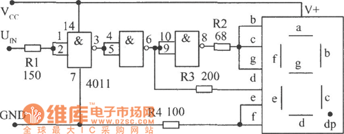
The level test circuit diagram composed of 4011 CMOS NAND gate connected as an inverter is shown as the chart. In this circuit, it can use NOT gate to instead of 4011. High level shows H, low level displays L. Since R2 ~ R4 has played the role of limiting current, the digital tube and its anode is connected directly with the positive power supply Vcc. The high, low level illuminated strokes e, f are connected to ground by R4, it may reduce the driving current.
Reprinted Url Of This Article:
http://www.seekic.com/circuit_diagram/Measuring_and_Test_Circuit/Level_test_circuit_diagram_composed_of_4011_CMOS_NAND_gate_connected_as_an_inverter.html
Print this Page | Comments | Reading(3)

Article Categories
power supply circuit
Amplifier Circuit
Basic Circuit
LED and Light Circuit
Sensor Circuit
Signal Processing
Electrical Equipment Circuit
Control Circuit
Remote Control Circuit
A/D-D/A Converter Circuit
Audio Circuit
Measuring and Test Circuit
Communication Circuit
Computer-Related Circuit
555 Circuit
Automotive Circuit
Repairing Circuit
Code: