Electrical Equipment Circuit
FAST_SAMPLE_AND_HOLD
Published:2009/7/20 21:42:00 Author:Jessie | From:SeekIC

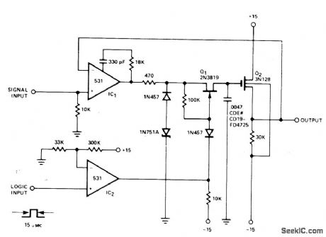
Strobe pulse developed from logic input of 531 opamp IC, turns on JFET Q1 to complete feedback loop to IC1, Q1, and Q2. C1 charges to voltage equal to that of input signal plus gate-to-source offset voltage of Q2. At end of strobe time, feedback loop is broken and C, holds voltage until time of next strobe pulse. Decay in output voltage between samplings is 1mV/s.- Signetics Analog Data Manual, Signetics, Sunnyvale, CA, 1977, p 643-644.
Reprinted Url Of This Article:
http://www.seekic.com/circuit_diagram/Electrical_Equipment_Circuit/FAST_SAMPLE_AND_HOLD.html
Print this Page | Comments | Reading(3)

Article Categories
power supply circuit
Amplifier Circuit
Basic Circuit
LED and Light Circuit
Sensor Circuit
Signal Processing
Electrical Equipment Circuit
Control Circuit
Remote Control Circuit
A/D-D/A Converter Circuit
Audio Circuit
Measuring and Test Circuit
Communication Circuit
Computer-Related Circuit
555 Circuit
Automotive Circuit
Repairing Circuit
Code: