Communication Circuit
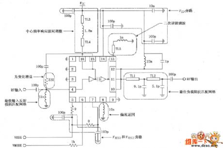
USA CDMA application circuit composed of RF2162
Published:2011/10/23 21:51:00 Author:May | Keyword: USA CDMA | From:SeekIC

The diagram is USA CDMA application circuit composed of RF2162. Radio-frequency signal (RF) isinput by pin 4, enlarged by preamplifier, final power amplifier, then output by pin 10, 11, 12. Pin 4 is directly coupling with inside amplifier, so itsuggests to add an UHF blocking coupling capacitor.Pin 13 is used as thesecond harmonics filter circuit, and it uses transmission line or inductanceandchip capacitor to make up filter with resonance at 2f0, it can offer low impedance path to second harmonics and short-circuit second harmonics effectively. Pin 14 is used as the final power amplifier power supply end, which offers bias current. Pin 5 connects to thefirst step enable voltage VREG1, when this pin is low level, the circuit shuts off; when it is inhigh level ( 2.8V),all circuit worksin thestandard state, and pin 5is connectedto 100pF high frequency filter capacitor. Pin 6 connects toanalog bias control pin VMODE, when pin 6 is 0V, itoffers theminimum bias.
Reprinted Url Of This Article:
http://www.seekic.com/circuit_diagram/Communication_Circuit/USA_CDMA_application_circuit_composed_of_RF2162.html
Print this Page | Comments | Reading(3)

Article Categories
power supply circuit
Amplifier Circuit
Basic Circuit
LED and Light Circuit
Sensor Circuit
Signal Processing
Electrical Equipment Circuit
Control Circuit
Remote Control Circuit
A/D-D/A Converter Circuit
Audio Circuit
Measuring and Test Circuit
Communication Circuit
Computer-Related Circuit
555 Circuit
Automotive Circuit
Repairing Circuit
Code: