Communication Circuit
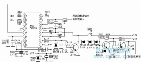
TA8859 pincushion correction circuit diagram
Published:2011/4/24 3:26:00 Author:Rebekka | Keyword: pincushion correction circuit | From:SeekIC

Field excitation pulse input
N402 (TA8859) 2 foot parabolic wave output voltage is amplified by the V401 ~ V403, and outputs the parabolic wave by V403 collector. It will be sent to the line deflection coil and change the flow through the line deflection coil current. That is, completion of the East / West pincushion correction. The east / west pincushion correction is sent to bus adjustment mode.
Pin 1: 3.7V-- high stability detection input Pin 2: 1.1V-- something the school pillows parabolic wave output Pin 3: 12.0V-- +12 V voltage input Pin 4: 5.5V-- something the school pillows feedback input side Pin 5: 0V - to Pin 6: 4.2V-- the input field scanning FeedbackPin 7: 0V Pin 8: 2.1V-- Field sawtooth voltage output Pin 9: 4.8V-- Bus cable connector Pin 10: 4.8V-- Bus clock line Pin 11 connector: 0V- - empty pin Pin 12: 0V - to Pin 13: 4.4V-- field excitation pulse signal input Pin 14: 3.8V-- external pulse shaping filter side Pin 15: 6.0V-- field scanning ramp voltage to form side Pin 16: 3.0V-- end automatic gain control filter
Reprinted Url Of This Article:
http://www.seekic.com/circuit_diagram/Communication_Circuit/TA8859_pincushion_correction_circuit_diagram.html
Print this Page | Comments | Reading(3)

Article Categories
power supply circuit
Amplifier Circuit
Basic Circuit
LED and Light Circuit
Sensor Circuit
Signal Processing
Electrical Equipment Circuit
Control Circuit
Remote Control Circuit
A/D-D/A Converter Circuit
Audio Circuit
Measuring and Test Circuit
Communication Circuit
Computer-Related Circuit
555 Circuit
Automotive Circuit
Repairing Circuit
Code: