Communication Circuit
10_MHz_FIBEROPTIC_RECEIVER
Published:2009/7/1 23:36:00 Author:May | From:SeekIC

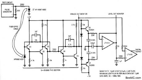
The receiver will accurately condition a wide range of light inputs at up to 10 MHz data rates.The optical signal is detected by the PIN photodiode and amplified by a broadband fed-back stage, Q1-Q3. A second, similar, stage gives further amplification.The output of this stage (Q5's collector) biases a 2-way peak detector (Q6-Q7). The maximum peak is stored in Q6's emitter capacitor while the minimum excursion is retained in Q7's emitter capacitor. The dc value of Q5's output signal's mid-point appears at the junction of the 0.005μF capacitor and the 22 M ohm unit. This point will always sit midway between the signal's excursions, regardless of absolute amplitude. This signal-adaptive voltage is buffered by the low bias LT1012 to set the trigger voltage at the LT1016's positive input. The LT1016's negative input is biased directly from Q5's collector.
Reprinted Url Of This Article:
http://www.seekic.com/circuit_diagram/Communication_Circuit/10_MHz_FIBEROPTIC_RECEIVER.html
Print this Page | Comments | Reading(3)

Article Categories
power supply circuit
Amplifier Circuit
Basic Circuit
LED and Light Circuit
Sensor Circuit
Signal Processing
Electrical Equipment Circuit
Control Circuit
Remote Control Circuit
A/D-D/A Converter Circuit
Audio Circuit
Measuring and Test Circuit
Communication Circuit
Computer-Related Circuit
555 Circuit
Automotive Circuit
Repairing Circuit
Code: