
Basic Circuit
Index 464
Low power consumption monostable circuit diagram
Published:2011/3/30 21:40:00 Author:Ecco | Keyword: Low power consumption, monostable

The circuitry shown as below, it includes a four 2 input port and NOT-gate CD4011 and a CMOS type 555, as a result whether it is inthe timing period of quiescent or high output level, it consumes very low. The portal 3 of CD4011, portal 4 constitute RS trigger. Because the whole circuitry presents in closed cycle, the pulse width is decided by the RC time constant, namely td=the 1.1 R1 C1.
(View)
View full Circuit Diagram | Comments | Reading(815)
tda2004 circuit diagram 2
Published:2011/3/30 21:31:00 Author:Ecco

tda2004 circuit diagram 2 is as below:
(View)
View full Circuit Diagram | Comments | Reading(997)
tda1521 Application circuit diagram
Published:2011/3/30 21:32:00 Author:Ecco | Keyword: Application

The Pinout function and referenced voltage of TDA1521:CSYN: 11V--inverted input 1(L sound channel input)VSYN: positive--going input 1VCH: 11V--consult 1(When OCL connection is 0V, OTL connection is 1/2 Vcc)SCK: 11V--output 1( L sound channel output)DI: 0V--negative electricity input(OTL connect to the earth)DO: 11V--output 2(R sound channel output)MON: 22V--positive electricity inputEXTCLK--positive-going input 2VCC--inverted input 2(L sound channel input) (View)
View full Circuit Diagram | Comments | Reading(2400)
The circuit diagram of TTL level displayed by LED
Published:2011/3/30 21:19:00 Author:Ecco | Keyword: TTL level, LED

This circuitry could be used to observe the TTL electrical level when there's no cathode-ray oscillograph . 74123 integrated circuit contains two trigger type of monostable harmonic oscillators with input of zero clearing, and they are marked as A1 andA2 in this circuit respectively. When the input level changes, the tmonostable harmonic oscillator will light more light emitting diode. Because single firm extended the pulse width, even if the input brain is very narrow, naked eye can still arguing the brightness of diode. The exhibit explains three light-emitting diodes mean of different states. (View)
View full Circuit Diagram | Comments | Reading(1544)
Ratio of the unknowns circuit diagram
Published:2011/3/29 20:11:00 Author:Ecco | Keyword: Ratio of the unknowns

This circuit is used as the situation of two signals share the same input line, for example, two leds irradiate a single photocell alternately. To measure the ratio of two unknowns, the precision better than 1%. During the period of T1, the input signal is sampled by S2, and storaged in C2, so that to make a comparison with reference voltage, the result of which can be obtained by the amplifier network AFE, added to gain control elements CLM6000. The adjusting signal gain of closed loop is increased, and the denominator of ratio is equal to reference voltage. And the molecular corresponding to T2 multiplied by the same gain, so the output of molecular direct ratio to the needed unknow value B/A .
(View)
View full Circuit Diagram | Comments | Reading(345)
CD4541 cadmium nickel storage cell recharger circuit diagram
Published:2011/3/29 20:01:00 Author:Ecco | Keyword: cadmium nickel storage cell , recharger

CD4541 cadmium nickel storage cell recharger circuit diagram is as below:
(View)
View full Circuit Diagram | Comments | Reading(1323)
The internal circuit diagram of crystal diode DM1500LFD5
Published:2011/3/29 2:52:00 Author:Ecco | Keyword: crystal diode

The internal circuit diagram of crystal diode DM1500LFD5 is as below:
(View)
View full Circuit Diagram | Comments | Reading(329)
The internal circuit diagram of crystal diode HZM27FA
Published:2011/3/29 2:51:00 Author:Ecco | Keyword: crystal diode

The internal circuit diagram of crystal diode HZM27FA is as below:
(View)
View full Circuit Diagram | Comments | Reading(418)
The internal circuit diagram of crystal diode HM5.6FA
Published:2011/3/29 2:49:00 Author:Ecco | Keyword: crystal diode

The internal circuit diagram of crystal diode HM5.6FA is as below:
(View)
View full Circuit Diagram | Comments | Reading(351)
The internal circuit diagram of crystal diode HZM6.8MFA
Published:2011/3/24 3:54:00 Author:Ecco | Keyword: crystal diode
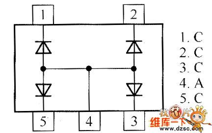
The internal circuit diagram of crystal diode HZM6.8MFA is as below:
(View)
View full Circuit Diagram | Comments | Reading(393)
The internal circuit diagram of crystal diode MMBD4448HADW
Published:2011/3/24 3:48:00 Author:Ecco | Keyword: crystal diode

The internal circuit diagram of crystal diode MMBD4448HADW is as below:
(View)
View full Circuit Diagram | Comments | Reading(402)
The internal circuit diagram of crystal diode MMBD4448HAQW
Published:2011/3/24 3:49:00 Author:Ecco | Keyword: crystal diode
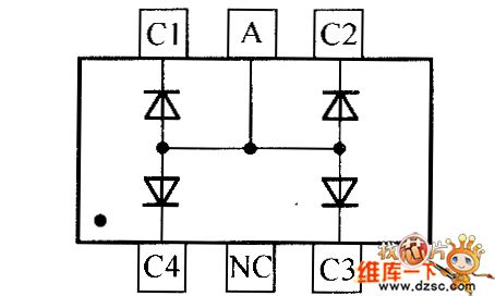
The internal circuit diagram of crystal diode MMBD4448HAQW is as below:
(View)
View full Circuit Diagram | Comments | Reading(405)
The internal circuit diagram of crystal diode MMBD4448HCDW
Published:2011/3/24 3:50:00 Author:Ecco | Keyword: crystal diode
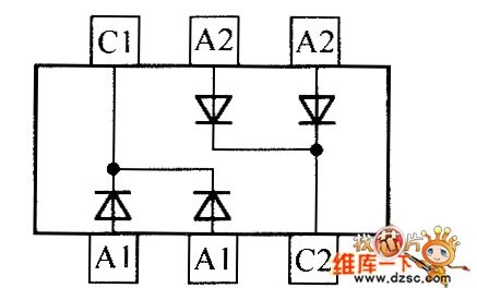
The internal circuit diagram of crystal diode MMBD4448HCDW is as below:
(View)
View full Circuit Diagram | Comments | Reading(334)
The internal circuit diagram of crystal diode MMBD448HCQW
Published:2011/3/24 3:51:00 Author:Ecco | Keyword: crystal diode
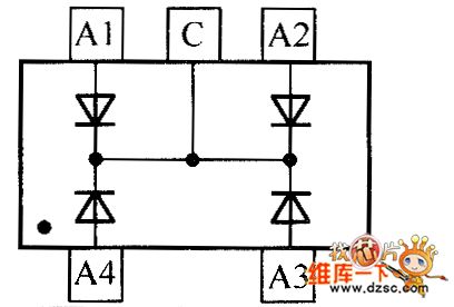
The internal circuit diagram of crystal diode MMBD448HCQW is as below:
(View)
View full Circuit Diagram | Comments | Reading(352)
The internal circuit diagram of crystal diode MMBD4448HSDW
Published:2011/3/24 3:51:00 Author:Ecco | Keyword: crystal diode

The internal circuit diagram of crystal diode MMBD4448HSDW is as below:
(View)
View full Circuit Diagram | Comments | Reading(350)
The internal circuit diagram of crystal diode MMBD4448HTW
Published:2011/3/24 3:52:00 Author:Ecco | Keyword: crystal diode

The internal circuit diagram of crystal diode MMBD4448HTW is as below:
(View)
View full Circuit Diagram | Comments | Reading(404)
Differentiator circuitry diagram
Published:2011/3/28 0:55:00 Author:Ecco | Keyword: Differentiator
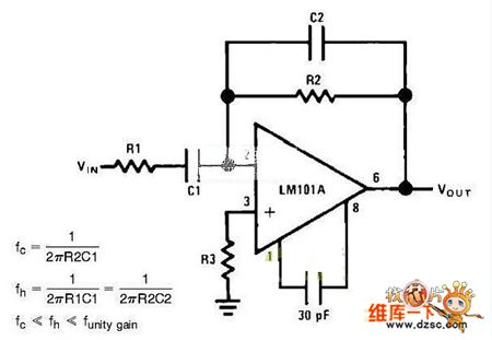
Differentiator circuitry diagram is as below:
(View)
View full Circuit Diagram | Comments | Reading(919)
Integrator circuit diagram
Published:2011/3/28 0:57:00 Author:Ecco | Keyword: integrator
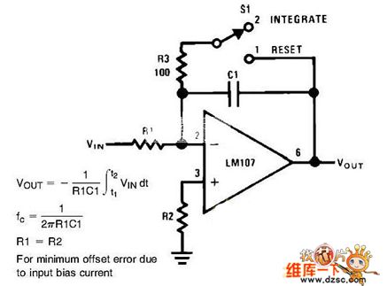
Integrator circuit diagram is as below:
(View)
View full Circuit Diagram | Comments | Reading(532)
The internal circuit diagram of crystal diode RKZ6.8MFAKT
Published:2011/3/28 0:58:00 Author:Ecco | Keyword: crystal diode

The internal circuit diagram of crystal diode RKZ6.8MFAKT is as below:
(View)
View full Circuit Diagram | Comments | Reading(359)
Binary to decimal system decoding circuit diagram
Published:2011/3/25 4:31:00 Author:Ecco | Keyword: Binary system, decimal system, decoding
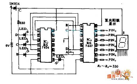
The PS7447 BCD code goes to 7 translators can provide 7 total anode figures display. With six inverter RS7404 and binary input indicator constituting of 4 LEDs means that the input takes binary types to represent decimal system 0~9; It's suitable for teaching experiment.
(View)
View full Circuit Diagram | Comments | Reading(3330)
| Pages:464/471 At 20461462463464465466467468469470471 |
Circuit Categories
power supply circuit
Amplifier Circuit
Basic Circuit
LED and Light Circuit
Sensor Circuit
Signal Processing
Electrical Equipment Circuit
Control Circuit
Remote Control Circuit
A/D-D/A Converter Circuit
Audio Circuit
Measuring and Test Circuit
Communication Circuit
Computer-Related Circuit
555 Circuit
Automotive Circuit
Repairing Circuit