Basic Circuit
TREBLE_BOOSTER_CIRCUIT
Published:2009/7/14 19:48:00 Author:May | From:SeekIC
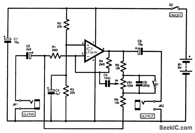
The circuit is basically a noninverting-mode amplifier. Resistors R2 and R3 bias IC1's noninverting input (pin 3), and R1 plus R4 act as a negative feedback network that sets the closed-loop volt-age gain of IC1 at unity. However, R1 and R4 are used only to set the operating conditions of IC1 at dc and at low to middle audio frequencies. The high-frequency voltage gain is governed by a more-complex negative feedback network that is composed of resistors R5 and R6, potentiometer VR1, and capacitors C4 and C6. R5, VR1, and R6 form a conventional negative feedback network that enables the voltage gain of the circuit to be varied. With the wiper (w) of VR1 toward the top end of its track, the circuit provides losses of nearly 20 dB. Moving the wiper down to the bottom gives almost 20 dB of gain. It is coupled to the inverting input via capacitor C4, which has quite a low value. Consequently, C4 provides an efficient coupling only at high frequencies. At middle and bass frequencies, capacitor C4 has a very high impedance and provides only a loose coupling to IC1's inverting input.Therefore, control VR1 is ineffective at these lower frequencies, where the voltage gain of the circuit is largely governed by resistors R1 and R4. This permits the required boost and cut to be obtained at high frequencies, but keeps the gain at about unity at middle and low
Reprinted Url Of This Article:
http://www.seekic.com/circuit_diagram/Basic_Circuit/TREBLE_BOOSTER_CIRCUIT.html
Print this Page | Comments | Reading(3)

Article Categories
power supply circuit
Amplifier Circuit
Basic Circuit
LED and Light Circuit
Sensor Circuit
Signal Processing
Electrical Equipment Circuit
Control Circuit
Remote Control Circuit
A/D-D/A Converter Circuit
Audio Circuit
Measuring and Test Circuit
Communication Circuit
Computer-Related Circuit
555 Circuit
Automotive Circuit
Repairing Circuit
Code: