Basic Circuit
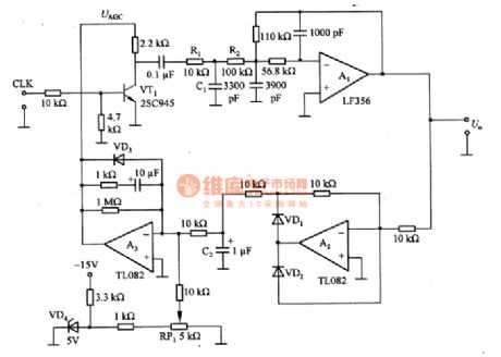
Sine wave output circuit composed of the TL082
Published:2011/8/24 21:30:00 Author:Christina | Keyword: Sine wave, output circuit | From:SeekIC

The sine wave output circuit which is composed of the TL082. The CLK is the input clock signal, it has the frequency division effect to the signal which is produced by the crystal oscillator and it changes the signal into the 1 kHZ clock signal. VT1 is the amplitude modulation circuit, we use the 1 kHZ clock signal to control the on/off of the control voltage UAGC to make it produce the square wave, and then we use the low-pass filter to filter out the higher harmonic. The R1 and C1 can be used to set the time constant of the rising edge of the square wave, the c=3~A (c is the cutoff frequency of the wave filter). in order to design the filter accurately, we can set the buffer amplifier A1 to isolate the R1 and R2.
Reprinted Url Of This Article:
http://www.seekic.com/circuit_diagram/Basic_Circuit/Sine_wave_output_circuit_composed_of_the_TL082.html
Print this Page | Comments | Reading(3)

Article Categories
power supply circuit
Amplifier Circuit
Basic Circuit
LED and Light Circuit
Sensor Circuit
Signal Processing
Electrical Equipment Circuit
Control Circuit
Remote Control Circuit
A/D-D/A Converter Circuit
Audio Circuit
Measuring and Test Circuit
Communication Circuit
Computer-Related Circuit
555 Circuit
Automotive Circuit
Repairing Circuit
Code: