Basic Circuit
RF_PROBE_1
Published:2009/7/9 20:57:00 Author:May | From:SeekIC

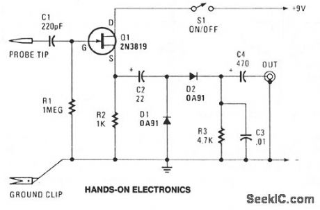
Transistor Q1-conftgured as a source-follower buffer stage, offering a bit under unity voltage gain-gives the unit a high-impedance input of about 1 MΩ shunted by about 10 pF, which keeps only minimal loading on the equipment being tested. C1 serves as input dc blocking capacitor. The Q1 output is coupled by C2 to a simple AM detector circuit made up of D1, D2, R3 and C3. Capacitor C4 provides output dc blocking. Total current consumption should be somewhere around 1 mA. The circuit responds to frequencies from 100 kHz to well over 50 MHz.
Reprinted Url Of This Article:
http://www.seekic.com/circuit_diagram/Basic_Circuit/RF_PROBE_1.html
Print this Page | Comments | Reading(3)

Article Categories
power supply circuit
Amplifier Circuit
Basic Circuit
LED and Light Circuit
Sensor Circuit
Signal Processing
Electrical Equipment Circuit
Control Circuit
Remote Control Circuit
A/D-D/A Converter Circuit
Audio Circuit
Measuring and Test Circuit
Communication Circuit
Computer-Related Circuit
555 Circuit
Automotive Circuit
Repairing Circuit
Code: