Basic Circuit
Platinum resistance signal conditioner ADT70 interior circuit diagram and typical application circuit diagram
Published:2011/4/21 21:40:00 Author:muriel | Keyword: Platinum resistance signal conditioner | From:SeekIC
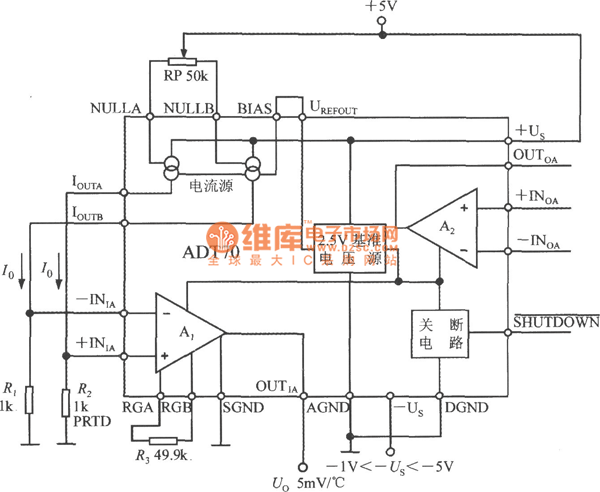
As shown is Internal circuit diagram and typical application circuit of platinum resistance signal conditioner ADT70. There are five parts of the chip:1. 2.5V reference voltage source2. two balanced output type current source3. instrument amplifier A14. reserve amplifier A25. turn-off circuit
In the picutre it uses the double-power supply. When -Us is at least -1V, it can measure the temperature below 0°C. The SGND、AGND and DGNA are all grounding. When SHUTDOWN non-connected the DGND, the ADT70 is turned-off; Without the end, it should be connected the +Us. When +5V power supply go through the potentiometer, it will supply the current source power. The 2.5V reference voltage sourceprovides bias to the current source. Two current source respectiveprovide exciting current for nominal resistance R1 and platinum resistance R2, The voltage difference of R2 and R1 is used for the input voltage of instrument amplifier. After adjust the gain of the instrument amplifier, It can obtain the output voltage Uo which vary directly as the measured temperature, final it send to the digital voltmeter that will show the measured temperature value. The resistence of R1 is 1KΩ. R2 is Pt1000 platinum resistance, its nominal resistence is 1kΩ below 0°C. RP is tone balance potentiometer. R3 is gain resistance of instrument amplifier.
Reprinted Url Of This Article:
http://www.seekic.com/circuit_diagram/Basic_Circuit/Platinum_resistance_signal_conditioner_ADT70_interior_circuit_diagram_and_typical_application_circuit_diagram.html
Print this Page | Comments | Reading(3)

Article Categories
power supply circuit
Amplifier Circuit
Basic Circuit
LED and Light Circuit
Sensor Circuit
Signal Processing
Electrical Equipment Circuit
Control Circuit
Remote Control Circuit
A/D-D/A Converter Circuit
Audio Circuit
Measuring and Test Circuit
Communication Circuit
Computer-Related Circuit
555 Circuit
Automotive Circuit
Repairing Circuit
Code: