Basic Circuit
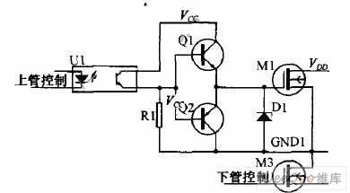
Optically Coupled High-side Driving Circuit of Improved Double Power
Published:2011/6/10 6:55:00 Author:Michel | Keyword: Improved Double Power, Optically Coupled, High-side, Driving Circuit | From:SeekIC

In the abboved double power coupling tube drive circuit scheme,using the copling output direct driving circuit makes the output waveform deformated seriously.Especially the falling edge of the waveform is slower, this is mainly caused by the capacitance between the MOS tube's G and S'level. The capacitance between G and s will be charged when the output waveform is high electricity ,which makes the wavefrom rise slightly slow.The capacitance between G and s will be discharged via R1 when the output waveform turns lower,which makes electric potential of MOS tube's G stage drop slowly and the wavform deformates seriously.It's impossible to remove the capacitance between G and s,we improve the mentioned driving project,according to pulling driving circuit on the thread on singlechip mouth and the imroving project is showed as above.
Reprinted Url Of This Article:
http://www.seekic.com/circuit_diagram/Basic_Circuit/Optically_Coupled_High_side_Driving_Circuit_of_Improved_Double_Power.html
Print this Page | Comments | Reading(3)

Article Categories
power supply circuit
Amplifier Circuit
Basic Circuit
LED and Light Circuit
Sensor Circuit
Signal Processing
Electrical Equipment Circuit
Control Circuit
Remote Control Circuit
A/D-D/A Converter Circuit
Audio Circuit
Measuring and Test Circuit
Communication Circuit
Computer-Related Circuit
555 Circuit
Automotive Circuit
Repairing Circuit
Code: