Basic Circuit
High_input_voltage_IC_filter
Published:2009/7/24 13:27:00 Author:Jessie | From:SeekIC
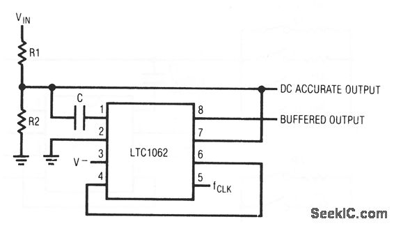
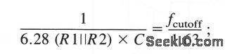
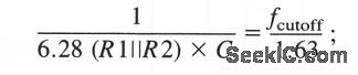
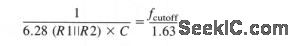
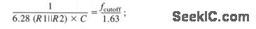
This circuit shows how an LTC1062 can be connected to accommodate high input voltages outside the normal input common-mode range. The dc gain of the low-pass filter is: R2/(R1 + R2). For maximum passband flatness, the paralleled combination of R1/R2 should be chosen as:
R1/R2≥ 5 kΩ. Notice that there is no need for an external op amp to buffer the divided-down input voltage. The internal buffer input (pin 7) performs this function. Linear Technology Corporation, Linear Applications Handbook, 1992, p. AN24-7.
Reprinted Url Of This Article:
http://www.seekic.com/circuit_diagram/Basic_Circuit/High_input_voltage_IC_filter.html
Print this Page | Comments | Reading(3)

Article Categories
power supply circuit
Amplifier Circuit
Basic Circuit
LED and Light Circuit
Sensor Circuit
Signal Processing
Electrical Equipment Circuit
Control Circuit
Remote Control Circuit
A/D-D/A Converter Circuit
Audio Circuit
Measuring and Test Circuit
Communication Circuit
Computer-Related Circuit
555 Circuit
Automotive Circuit
Repairing Circuit
Code: