Basic Circuit
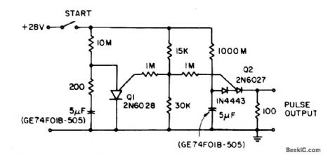
HOUR_TIME_DELAY_SAMPLING_CIRCUIT
Published:2009/7/7 3:29:00 Author:May | From:SeekIC


The circuit lowers the effective peak current of the output PUT, Q2. By allowing the capacitor to charge with high gate voltage and periodically lowering gate voltage, when Q1 fires, the timing resistor can be a value which supplies a much lower current than Ip. The triggering requirement here is that minimum charge to trigger flow through the timing resistor during the period of the Q1 oscillator. This is not capacitor size dependent, only capacitor leakage and stability dependent.
Reprinted Url Of This Article:
http://www.seekic.com/circuit_diagram/Basic_Circuit/HOUR_TIME_DELAY_SAMPLING_CIRCUIT.html
Print this Page | Comments | Reading(3)

Article Categories
power supply circuit
Amplifier Circuit
Basic Circuit
LED and Light Circuit
Sensor Circuit
Signal Processing
Electrical Equipment Circuit
Control Circuit
Remote Control Circuit
A/D-D/A Converter Circuit
Audio Circuit
Measuring and Test Circuit
Communication Circuit
Computer-Related Circuit
555 Circuit
Automotive Circuit
Repairing Circuit
Code: