Basic Circuit
EFFICIENT_POWER_BOOSTER
Published:2009/7/9 23:50:00 Author:May | From:SeekIC

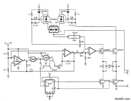
This power booster functions as a high-efficiency power multiplexer or, if you supply an external signal-source, as a high-power linear amplifier.
If you want to drive a load with a high-power square wave, the circuit simply draws power from two external power sources, V1 and V2, alternately. In this mode, the circuit's power-handling devices func-tion as switches, dissipating minimal power. The RC time constant of the integrator,IC1, determines the circuit's oscillation period.
If you supply an external drive waveform, the circuit functions as a linear amplifier,and,consequently, inherently dissipates varying portions of that power. The power amplifier is stable for gains ≥15.
Diodes D1 and D2 limit the FET's gate-voltage swing to less than 15 V. D3 is a dual Schottky diode that protects the FETs from short circuits between the two supplies, V1 and V2, through a FET's para-sitic diode. With D3 in place, you can choose either power channel for the higher voltage input. To drive the FETs, Q5 and Q6, at switching frequencies greater than 1 KHz, you will have to use gate drivers for them.
Reprinted Url Of This Article:
http://www.seekic.com/circuit_diagram/Basic_Circuit/EFFICIENT_POWER_BOOSTER.html
Print this Page | Comments | Reading(3)

Article Categories
power supply circuit
Amplifier Circuit
Basic Circuit
LED and Light Circuit
Sensor Circuit
Signal Processing
Electrical Equipment Circuit
Control Circuit
Remote Control Circuit
A/D-D/A Converter Circuit
Audio Circuit
Measuring and Test Circuit
Communication Circuit
Computer-Related Circuit
555 Circuit
Automotive Circuit
Repairing Circuit
Code: