Basic Circuit
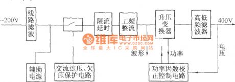
DZW75-48/5050II power factor compensation
Published:2011/12/4 20:50:00 Author:May | Keyword: power factor compensation | From:SeekIC


The elementary diagram of DZW75-48/5050II power factor compensation:
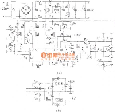
DZW75-48/5050II power factor compensation circuit:
In the diagram, (a) is compensation circuit, (b) is auxiliary power supply. It mainly consists of N1, power factor calibration control module and some support circuits. N1 internal circuit consists of saw-tooth wave generator, pulse width modulator and multiple comparator circuit and so on. The frequency of saw-tooth wave generator is determined by out-connected capacitor and resistor. This machine makes the frequency of its output pulse work at 50 kHz, and the width of output pulse is determined by the error voltage after a general comparison treatment. It has three sampling and comparison circuits. V6 is actually an integrated chip containing VMOS tube,enhance diode and rectifier bridge.
Reprinted Url Of This Article:
http://www.seekic.com/circuit_diagram/Basic_Circuit/DZW75_48_5050II_power_factor_compensation.html
Print this Page | Comments | Reading(3)

Article Categories
power supply circuit
Amplifier Circuit
Basic Circuit
LED and Light Circuit
Sensor Circuit
Signal Processing
Electrical Equipment Circuit
Control Circuit
Remote Control Circuit
A/D-D/A Converter Circuit
Audio Circuit
Measuring and Test Circuit
Communication Circuit
Computer-Related Circuit
555 Circuit
Automotive Circuit
Repairing Circuit
Code: