Basic Circuit
Basic timing circuit diagram formed by NE555
Published:2011/8/27 1:33:00 Author:Nancy | Keyword: Basic timing | From:SeekIC


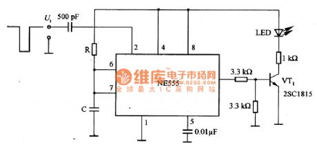
Figure 1 is the basic timing circuit diagram formed by NE555. Figure 1 (a) is the basic timing circuit diagram formed by NE555. In the circuit, if a trigger pulse is added to the pin 2 as shown in the figure 1, then there must be a certain time interval pulse in pin 3 output, the interval is T ~ RC, which is amplified by VT1 to drive the light-emitting diode LED in the related circuit in Figure 1.
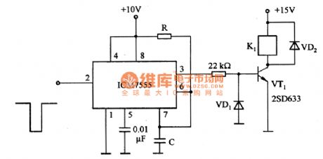
Figure 1 (b) is the timing circuit formed by CMOS (ICM7555). It adopts CMOS and has high impedance, the setting time can be greatly extended, for example, it can be used in the timer of a few minutes. In the figure, R is ranging from lkΩ to lOOMΩ, C is ranging from 1OOpF to 10000μF.
Reprinted Url Of This Article:
http://www.seekic.com/circuit_diagram/Basic_Circuit/Basic_timing_circuit_diagram_formed_by_NE555.html
Print this Page | Comments | Reading(3)

Article Categories
power supply circuit
Amplifier Circuit
Basic Circuit
LED and Light Circuit
Sensor Circuit
Signal Processing
Electrical Equipment Circuit
Control Circuit
Remote Control Circuit
A/D-D/A Converter Circuit
Audio Circuit
Measuring and Test Circuit
Communication Circuit
Computer-Related Circuit
555 Circuit
Automotive Circuit
Repairing Circuit
Code: